“Bringing integrated photonics to daily life”

PITC Metrology programme - Sylwester Latkowski, PITC (left), Jan Mink, VTEC (right)
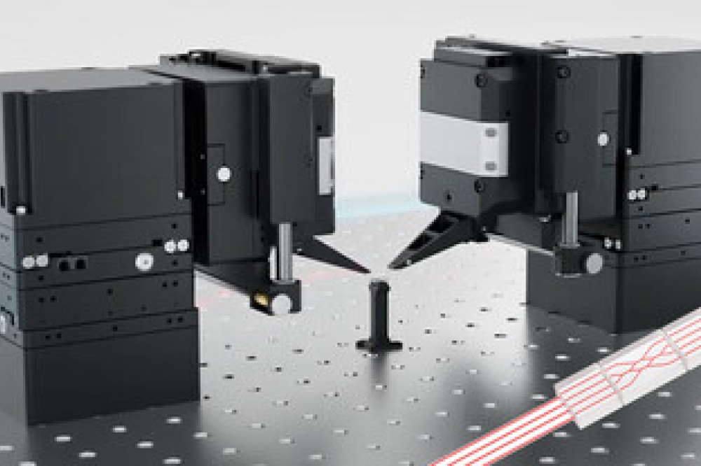
Integrated photonics will have a sustainable impact on society, but its adoption is hampered by long product development cycles and limited production throughput. Improving and scaling measurement and test technology are crucial for accelerating the uptake of integrated photonics. To address these challenges, the Photonic Integration Technology Center has launched the Metrology program, aimed at developing design-for-test methodologies and new product characterization and test automation tools. The program consortium includes integrated photonics designers, manufacturers, and product suppliers, as well as automated test equipment suppliers. The program kicked off with an official starting event last September, and is still open to (international) companies that wish to join a neutral platform for photonics metrology development.
Our world runs on micro-electronics, used in operating computers and controlling myriads of other devices and equipment, from smartphones and household appliances to cars and machines. Their performance and energy efficiency can be further enhanced by combining electronics with photonics (light technology), and integrating these technologies into complete packages and modules. This would result is the convergence of the upcoming photonics industry with the established semiconductor industry. Photonic integrated chips can increase the bandwidth of tele- and data-communication enormously, and enable innovative, light-based sensing applications. Integrated photonics will have grown into a multi-billion market by the year 2025, helping to solve some of society’s biggest challenges, ranging from energy-efficient communication and data handling to health monitoring. Founded in the world-leading Dutch photonics ecosystem, the Photonic Integration Technology Center (PITC) aims to accelerate the uptake of integrated photonics by bridging the divide between research and application.
Improving test processes
The main barriers for the market adoption of integrated photonics – a long time-to-market and a limited throughput in photonic chip production – can be attributed to a number of factors. Firstly, the development cycle is too long because new designs require verification and optimization through characterization. The number of tests required to stabilize a process and increase throughput is relatively high. Therefore, testing processes must improve in accuracy, reliability, throughput/speed, and cost-efficiency, explains Sylwester Latkowski, scientific director of PITC. “There is an urgent need to improve the scalability of the currently available test solutions, to facilitate an efficient process from the prototyping to the pilot phase, and to production in small batches and ultimately large volumes. Regarding the challenges in integrated photonics, a shift can be observed from the design phase to the assembly, packaging, and testing phases, which together account for 70-80% of the production cost, but which have until recently been overlooked by many parties. Testing will be crucial in gaining the market’s confidence in the expected yield and performance of photonic devices.”
Tenfold throughput increase
PITC took the initiative to start a Metrology program in order to address the challenges of lowering the barriers for market adoption and increasing market confidence. The program is aimed at developing design-for-test methodologies and new product characterization and test automation tools. “Our ambition is to reduce product development cycles by three months through enabling ‘right first time’ design, thus preventing unnecessary and costly design iterations,” states Latkowski, who is also acting Metrology program lead. “New test tools will help to drastically increase testing throughput. Depending on the complexity of the photonic product to be tested, the throughput on average has to increase from minutes to seconds per device. If this proves to be out of reach, then massively parallel testing procedures can serve as an alternative. Overall, we are striving for a throughput increase by a factor of ten. Production flow data analysis can also contribute to this.”
Customized systems
VTEC Lasers & Sensors, located in Eindhoven, is one of the program’s consortium partners. VTEC is an innovation solutions company that specializes in the integration of optics and data to create customized systems for a wide variety of industries, including telecommunication, manufacturing, environmental, and free-space communication. CEO Jan Mink explains, “We design chips for a wide range of applications, from transceivers for 5G communication to partially light-based multi-sensors for building automation. Test and measurement are among our biggest challenges. We employ dedicated test engineers, and our designers also engage in testing, to tailor their designs to the customer’s requirements and prevent production losses.”
Predictive test methods
Many product characteristics can be measured in the lab, Mink continues, “But in production we need a simple indicator that tells us whether we will have a sellable or an unsellable product. When we can take accurate measurements that give a good prediction for the final product quality early on, we can prevent the costly manufacturing and packaging steps for products that fail once packaged.” Metrology helps to increase the yield of chips, Latkowski confirms. “With adequate testing sequences and procedures in place, you can perform efficient design and prototyping iterations to bring the production process to the expected target quickly.” Mink adds, “We need predictive test methods, with the proper test equipment at the right cost, to take the step from small to large volumes with high reliability. This is exactly the subject of the work package we are leading. This program offers us a platform for exploring various test technologies, for example to reduce test time and extend our measurements to the 100 Gbit/s range, and getting to know the photonics supply chain.”
Learning from electronics testing
The Metrology program’s consortium includes experts in electronics testing and suppliers of automated test equipment. Latkowski explains that these companies can expand their portfolio of test systems into integrated photonics, by learning about new types of signals and materials. “In this way, they can benefit from the program, while their expertise in electronics testing will benefit the photonics companies because the semiconductor technologies are thirty years ahead in terms of high-throughput, large-volume production. Together, the partners can work on developing new test procedures, for example in the packaging and assembly processes, for the integration of electronics and photonics.”
Impact
The technological achievements of the Metrology program will have a direct economic impact, Latkowski declares. “Reducing development time and improving test throughput will contribute to an accelerated market introduction and a ramp-up of integrated photonics.” Ultimately, this will have an effect on society, Mink adds. “In our private and professional lives, tele- and data-communication are very important and we are using more and more bandwidth, leading to an increased power consumption by electronics-driven data centers. With integrated photonics, this trend can be reversed, which is crucial in the energy transition the world is facing right now.” Latkowski adds, “Integrated photonics will penetrate into our daily lives.”
Talent development
As well as applied research, the Metrology program also has a focus on talent development in order to address the shortage of technically skilled people who are familiar with integrated photonics design, manufacturing, and application. A collaboration has been set up with Eindhoven-based Fontys University of Applied Sciences to train engineers in photonics and install an internship program for six-month projects at companies. “This offers a steep learning curve for the students and good results for the companies,” Latkowski claims. “For example, Salland Engineering has started to upgrade the photonic skills of their staff.” The talent development commitment has already paid off, Mink adds. “We now have three students from Fontys working on photonics projects.”
International invitation
The Metrology program is still open to interested companies, Latkowski says. “This successful start has shown that there is a need for a neutral platform for technology development, where partners can decide what makes sense to share with others and what has to stay confidential because it defines their uniqueness. The participation of FiconTEC from Germany and APEX Technologies from France demonstrates that the program fills a need that is felt internationally. From a global perspective, the Metrology program is definitely a forerunner, as I concluded from my participation in the integrated photonic systems roadmapping activity at PhotonDelta and MIT Microphotonics Center, where we engaged with photonic communities around the globe.”
About the Metrology program
The Metrology program is PITC’s first large shared research program, bringing together integrated photonics designers (BRIGHT Photonics), photonic chip manufacturers (SMART Photonics), photonic product suppliers (VTEC and PhotonFirst), and automated test equipment suppliers (Salland Engineering, FiconTEC, and APEX Technologies). The program has a multiyear outlook and a launching budget of around five million euros, provided by PhotonDelta and the participating companies on an equal basis. A yearly review offers the industry partners the opportunity to adjust the course of the program. In addition, the budget can be augmented following PITC’s efforts to secure its financial basis by applying for funding from the European REACT-EU program and from the Dutch Growth Fund through the NextGen Hightech and PhotonDelta investment programs.
Companies that are interested in joining the program can contact PITC business development manager Jan-Laurens van der Steen, at jan-laurens.vandersteen@pitc.nl.


