Loading...
News Article

EVG unveils EVG150 resist processing system
News

Redesigned 200-mm platform increases module capacity for higher throughput

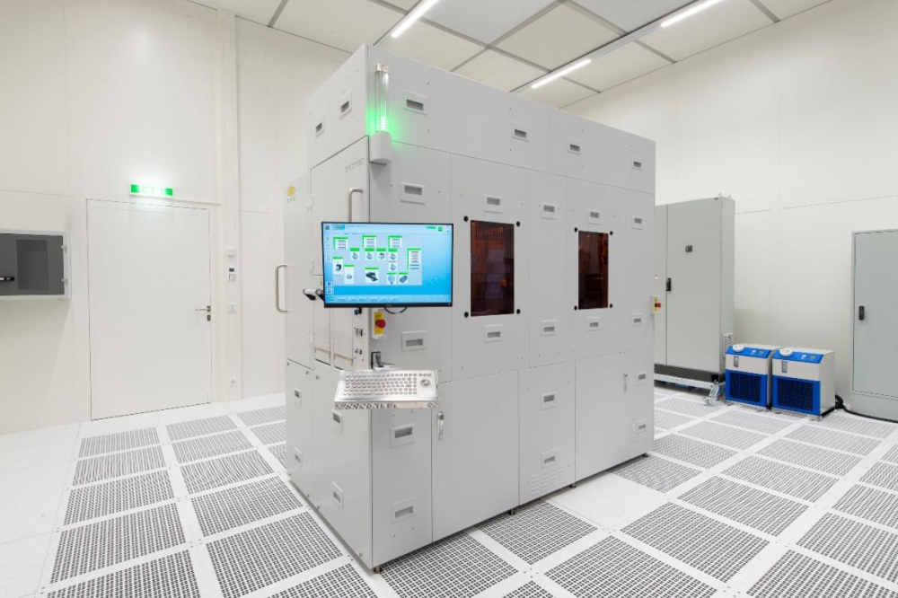
EV Group (EVG), a supplier of wafer bonding and lithography equipment, has unveiled the next-generation 200-mm version of its EVG150 automated resist processing system.

The redesigned EVG150 platform includes advanced features and enhancements that provide greater throughput (by up to 80 percent) and versatility, as well as smaller tool footprint (by nearly 50 percent), compared to the previous-generation platform.

The EVG150 is said to provides reliable and high-quality coating and developing processes in a universal platform that supports a variety of devices and applications, including advanced packaging, MEMS, radio frequency (RF), 3D sensing, power electronics, and photonics.

Silicon Austria Labs, a research centre, is the first customer to receive the next-generation EVG150 system. “Through our cooperative research with leading manufacturers, we develop key tech­nolo­gies that build the foundation for Industry 4.0, IoT, autonomous driving, cyber-phys­ical systems (CPS), AI, smart cities, smart energy, and smart health long before they reach the market,” stated Dr. Mohssen Moridi, Head of Research Division Microsystems of Silicon Austria Labs. “The high flexibility of EVG’s next-generation EVG150 resist processing system helps pave the way for high-volume implementation of new processes and products with our development customers that fuel EBS innovation.”

Company executives will be available to discuss the EVG150 resist processing system at SEMICON Europa, taking place next week at the Messe München in Munich, Germany, from November 15-18 (co-located with Electronica).


Quintessent appoints Bob Nunn chief operating officer
PI to demonstrate new PIC alignment system at Photonics West
Drut launches 2500 product series with CPO for AI datacentres
III-V Epi advocates GaAs for new lasers
Marvell announces new CPO architecture for custom AI accelerators
Printing high-speed modulators on SOI
Photon IP raises €4.75m for advanced PICs
ANELLO Photonics launches Maritime Inertial Navigation System
Aeluma joins AIM Photonics as full industry member
Imec makes breakthrough with GaAs lasers on silicon
POET acquires Super Photonics Xiamen
Voyant Photonics launches affordable Carbon LiDAR
Penn State makes breakthrough in photonic switching
New nanocrystals could lead to more efficient optical computing
QCi awarded NASA contract to apply Dirac-3 photonic optimisation solver
The Netherlands launches ChipNL Competence Centre
TOPTICA to create chip-integrated lasers for quantum PIC project
NSF selects six pilot projects for National Quantum Virtual Laboratory
SiLC Technologies launches Eyeonic Trace Laser Line Scanner
Southwest Advanced Prototyping Hub awarded $21.3 million CHIPS Act funding
Cambridge Graphene Centre and CORNERSTONE to participate in PIXEurope
Cost-effective lasers for extended SWIR applications
IBM unveils co-packaged optics technology for AI and datacentres
QCi announces $50 million concurrent stock offerings
CHIPS Act funding to be awarded to Coherent, Skywater, and X-Fab
ERC consolidator grant awarded for optoacoustic neural network project
Imec demonstrates InP chiplet integration on 300 mm RF silicon interposer
Ayar Labs raises $155 million for optical I/O
Celestial AI awarded 2024 Start-up to Watch by Global Semiconductor Alliance
Researchers develop “last missing piece” of silicon photonics
Quantum sensors for controlling prosthetics
UPVfab to participate in European Commission photonic chips project

×
Search the news archive

To close this popup you can press escape or click the close icon.
Logo
x
Logo
×
Register - Step 1

You may choose to subscribe to the PIC Magazine, the PIC Newsletter, or both. You may also request additional information if required, before submitting your application.


Please subscribe me to:


You chose the industry type of "Other"

Please enter the industry that you work in: