Nanometre components require sub-nanometre precision

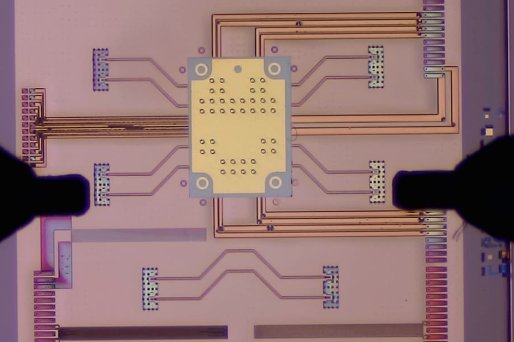
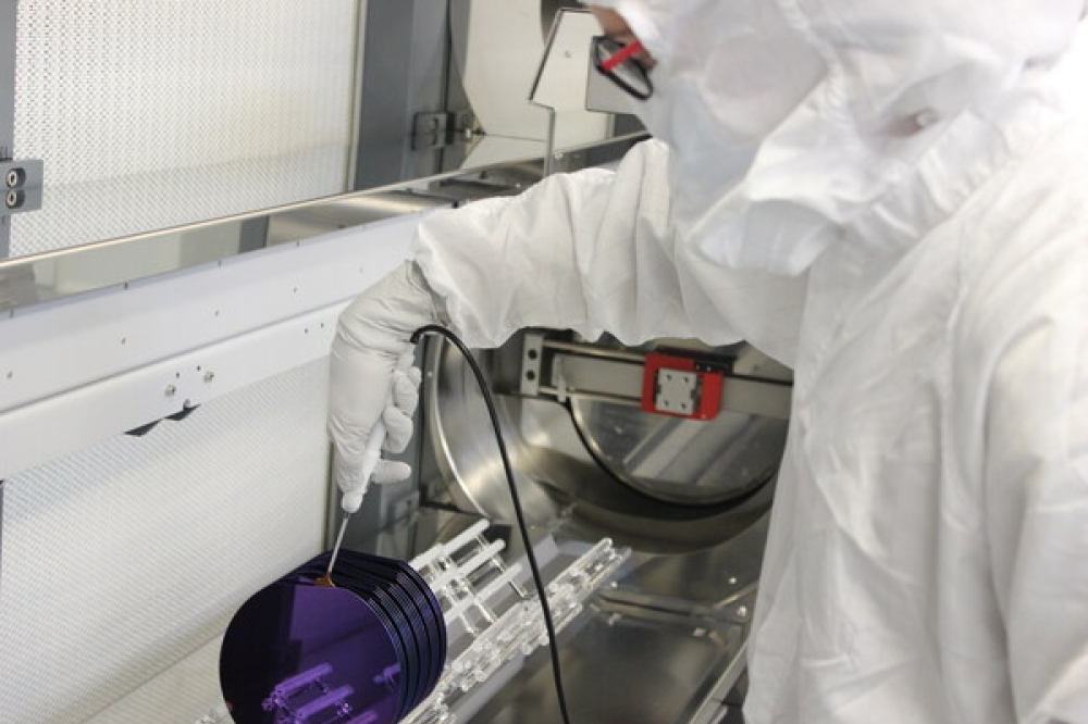
Semiconductors are an integral part in most electronic devices, and the racehorse in the charge towards greater computing power. Without these tiny components, we would not have been able to enjoy our smartphones and hyper-realistic video games. Semiconductors have evolved tremendously since they were first developed; as more and more computing power is sought after, the silicon chips shrink in size and, today, the smallest wafers are just 2 nm – a fraction of the width of a strand of DNA. Smaller chips means that the distance the electrons need to travel is decreased, allowing much faster processing. Unfortunately, it makes both the manufacturing and validation processes extremely difficult.
Time is money
Since semiconductors are necessary in virtually all types of
technology, they are constantly in high demand, and it is important that the
manufacturing process is efficient. A single chip can take a month to
manufacture and, depending on the design, the process can consist of 1,000 to
2,000 steps. It is common to check the device for faults between processing
steps, since moving to the end phase of the manufacture would be a waste of
time and money if the semiconductor has a defect.
Challenges at every step
Scanning semiconductors for flaws requires extremely
accurate motion control. As precision cannot come at the cost of speed, the
system must be able to move from point A to point B as quickly as possible.
Ideally, the motion will start instantaneously after the command has been
given, and come to a full stop as soon as the exact position has been reached.
In addition, when used in dynamic processes, for example when measurements are
performed during movement, the inspection head needs to be triggered at exactly
the right spot. However, in practice, there will always be some latency – a
delay before the inspection head is activated, and some settling time before
the motion of the stage stops completely. There will also be some positioning
inaccuracy, especially during acceleration. This latter issue can be affected
by many factors, such as flaws in position feedback system or drive mechanism,
or guidance errors in the bearings. Another common issue is vibrations caused
by the movement of the stage. These interferences will disturb the system and,
if the vibrations occur at one of the natural frequencies of the appliance,
they will be amplified. One way to fix this issue is to make the system as
stable and robust as possible, but these disturbances are hard to remove completely
during fast movements.
Innovative motion control powered by smart software
ACS Motion Control is a global supplier of motion control
systems, including controllers, motor drives, specialised IOs and various smart
software tools. The company was founded in Israel in 1985, and has since spread
all over the world – with offices in the USA, Germany, China and Korea – and
joined the Physik Instrumente (PI) group in 2017. ACS’s products are used in a
range of applications that require high precision motion control, from
optical-, ultrasonic- and e-beam inspection to X-ray, dimension metrology and
maskless lithography.
Software that can learn
ACS’s high performance motion solutions are powered by
intelligent software that helps the hardware to perform at its best. Its
patented NanoPWM technology uses both PWM- and linear power amplifiers,
allowing the stage to move at high speed and settle in nanometre-sized windows.
The MotionBoost algorithm creates motion profiles aimed at minimising vibration
and settling times, by reducing the energy supplied to the stage through
friction or moving parts. The effects of disturbances are further reduced by
the ServoBoost software, which works in real time to identify and compensate
for perturbations caused by cogging, load changing and cross-axis interactions.
This ensures faster settling, lower jitter and decreased dynamic error compared
to standard PID-based algorithms. The newest addition to the ACS portfolio is
LearningBoost, a state-of-the-art control algorithm that can not only sense and
cancel out disturbances, but also predict them, by learning the way the system
performs and which movements usually cause perturbations. Coupling
LearningBoost with the other software packages from ACS will enable previously
unachievable throughput and accuracy, making a huge difference for applications
such as semiconductor production that rely on high-precision motion control.
PI in brief
PI (Physik Instrumente), headquartered in Karlsruhe, is the
market and technology leader for high precision positioning technology and
piezo applications in the semiconductor industry, life sciences, photonics, and
in industrial automation. In close cooperation with customers from all over the
world and for 50 years now, PI's specialists (approx. 1,300) have, again and
again, been pushing the boundaries of what is technically possible and
developing customized solutions from scratch. More than 350 granted and pending
patents underline the company's claim to its leadership. PI has six production sites
and 15 sales and service offices in Europe, North America, and Asia.


