

Move PIC testing from lab to fab seamlessly
Automating PIC manufacturing processes including test,
assembly and packaging (TAP) are key to increasing product quality as
well as dramatically reducing overall production costs. The experts at
EXFO detail ways that automation continues to accelerate time to market
for PICs while helping reassure customers of consistent quality.
By François Couny, PhD, Senior Product Line Manager at EXFO
Mass production of photonic components requires fast, flexible, and integrated testing and characterization. And testing constitutes a big chunk of component manufacturers’ investment given that an estimated 30 percent of the total cost of photonic chip production is driven by testing.
Recent Photonic Integrated Circuits (PIC) testing advances have helped reduce operating expenses via increased speed, reliability, and scalability. PIC measurement can now be optimized using turn-key solutions – delivered through vendor collaborations -- to perform multiple tasks efficiently with easy reconfiguration. And new technologies are on the horizon to provide even more opportunities to reduce component manufacturing costs.
This article looks at the current state of PIC testing, progress made in seamlessly moving PIC testing from the lab to fabrication, and the advancements in laser technology that will reduce the cost and time of testing while maintaining reliability.
Streamlining the PIC testing process
Testing PICs has always been a big challenge over the decades of development in the cleanroom. Often researchers would put together some test instruments and perform the characterization by hand or even design their own dedicated instrument that could also include post-processing and analysis of the results. Over the past few years, test instruments designer EXFO has worked closely with these researchers to create instruments that are fine-tuned to the technical requirements of PIC optical testing.
Moving PIC-based passive component testing into production is often challenging due to the high port count of some components like arrayed waveguide grating (AWG) or the sheer number of components to test on a single die. Since testing requirements are very similar in the lab and in production of these specialized devices, component manufacturers can now use the same component test platforms they used during the development of the product in the factory. The test solution serves as a multiport detection system that operates in conjunction with a continuously tunable laser to measure optical insertion loss, return loss, and polarization-dependent loss across the laser’s spectral range. This cost-effective method yields optical spectrum quickly and with a high wavelength resolution down to a picometer level.

The CTP10 system can also be used with a matrix switch MXS-9100 for easy reconfiguration of PIC die-level testing as in this demonstration from Aerotech, EHVA, and EXFO
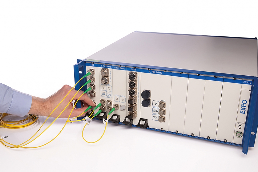
One further paradigm when considering testing in production is the need to reduce testing costs and hence reduce testing time. In the case of spectral measurement, the test consists of a laser performing a wavelength sweep and in synchronous detection of optical power onto one or several detectors. How much can be gained in speed comes down to how fast the laser can sweep, how quickly the detector can react to the change in optical power, and how long it takes for the data to become available to the operator.EXFO’s CTP10 is a modular component test platform that characterizes the spectral properties of high port count devices in one single scan with picometer resolution and a 70 dB dynamic range, even at high laser sweep speeds. The CTP10 operates from 1240 to 1680 nm and covers a wide range of test applications, including telecom, waveguide technology and coupling, sensing, and LIDAR.
The CPT10’s electronics and internal processor streamline data transfer as well as providing a suite of analysis tools, hence offering a solution that is fast in all aspects of the testing phase. Indeed, precious seconds per die can be gained by using such an integrated solution. On a wafer with several hundreds of dies, that is hours of testing that can be saved by using the CTP10.
EXFO’s CTP10 component testing platform can be configured for spectral testing of insertion loss, return loss, or polarization-dependent loss, of optical components such as ring resonators. The component testing platform can be controlled remotely using SCPI commands, enabling integration as part of an automated PIC testing setup, increasing PIC testing throughput while reducing test time. This is a key solution to measure optical components quickly, reliably, and accurately.
Automation to enable mass component production
When testing hundreds or even thousands of components on a single wafer, optimizing the automation process quickly becomes essential. This is particularly true because optical functionalities to be tested may vary from device to device or from die to die. As a result, PIC test solutions need to address fast reconfiguration of both software and hardware through the use of optical switches. Additionally, faster single-wavelength tests may also be beneficial at some points in the production process such as fiber alignment or after dicing. These simpler tests also help the overall speed of the test and measurement (T&M) process.
EXFO has addressed these challenges with a two-pronged approach. First, the FTBx series of modules provide the optical testing building blocks for a simple laser + power meter test configuration, with ample possibilities for adding attenuators, switches, or different types of optical sources. Second, the MXS matrix switch addresses the need for quick but repeatable reconfiguration, switching in a fraction of a second to a new configuration.

EXFO’s CTP10 system can be used with the wafer-level probe station from MPI Corporation
Supporting process design kits (PDKs)
Design and manufacturing of PIC dies is maturing fast, with photonic wafers now containing thousands of components made available by foundries through process design kits (PDKs). To create and update these PDKs, wafer manufacturers require reliable testing solutions to optimize the different parameters of interest for a given optical component. Ring resonators have attracted a lot of attention in recent years and are commonly found in PIC designs to create extremely narrow peaks/troughs that can be used, for instance, as modulators; however, they are notoriously difficult to characterize spectrally.
Testing is a crucial step after design and manufacturing to provide feedback to the design tools and help optimize them. It is also needed for process control, to ensure that devices operate as expected throughout the assembly and packaging of the PIC chips. The PIC devices are usually tested at the wafer level prior to dicing so as to detect defects as early as possible and to avoid packaging defective dies.
The ultimate goal of these PDKs is to allow the complete simulation of optical properties of a PIC design even before it is produced. However, ‘real’ testing will still remain in place in the lab for development of new components as well as in production to verify the specifications of the finished product.
Multi-vendor collaboration to deliver optimized solutions
It’s notable that when thinking about test solutions for PIC production, one should not limit the discussion to the testing itself. Indeed, light first needs to be coupled in and out of each device and that operation also needs to be as fast as possible. For that purpose, PIC wafer probe stations include specially-designed optical fiber hardware and high-precision alignment software. It is also possible to couple several components simultaneously using a fiber array. Precision alignment and speed allow coupling optimization within a fraction of a second. Once the light is coupled into the wafer, the optical characteristics of the device under test can be measured.
To create customized solutions supporting specific production requirements, EXFO is involved in key collaborations with industry leaders in the PIC ecosystem to validate hardware and software interoperability. Collaborating with major suppliers of high-accuracy wafer positioners such as MPI Corporation, Aerotech, and FormFactor ensures optimal performance of the overall test solution.
A recent example is the collaboration between Aerotech, EHVA and EXFO in demonstrating an automated integrated photonic test solution that accelerates the lab to production timeline. Photonics testing software seamlessly integrates with EXFO’s CTP-10 and Aerotech’s ultra-high precision photonics aligners, delivering optimum reliability and efficiency. EXFO’s PIC testing solutions can be fully automated and operated with third-party software integrators such as EHVA, OptiInstrument, and Maple Leaf Photonics (MLP) to provide turnkey solutions.
Next steps in PIC testing from lab to production
Clearly, several avenues can be investigated to ensure PIC component manufacturers are well equipped for mass production. First, testing speed needs to be pushed to the limit. Twice the scanning speed on the tunable laser, coupled with suitable detecting speeds, can reduce the overall test process by a factor of 2 if the data post-processing is also optimized. Second, rational testing needs to be implemented when possible, using reconfigurable hardware and software or even using PDKs to achieve “by-design” specifications. Lastly, the handling of data and results as proposed by companies such as EHVA will also become a key component of optical testing. What is certain is that the optical testing of PICs is set to evolve faster in the next few years than it has over the past decade, making ‘lab to fab’ a more seamless transition.
Visit https://www.exfo.com/en/solutions/academic-research-institutions/pic-testing/ for more information about EXFO’s PIC testing solutions.


