

Europe pilots PIC production
Producing photonic integrated circuits (PICs) at industrial
scale is a growing capability across the EU thanks to multiple EC-funded
programmes that seek to create a complete PIC ecosystem within Europe’s
borders. Taking a new product to the pilot line stage is one of the
last major steps toward commercialization. EPIC details recent advances
and the important role Indium Phosphide technologies will play in this
growing industry.
By: IVAN NIKITSKIY, PROGRAM MANAGER, PHOTONICS TECHNOLOGIES, EUROPEAN PHOTONICS INDUSTRY CONSORTIUM (EPIC)
Photonic integrated circuits (PICs) can be built on several material platforms that are complementary in many ways, but are also currently competing. The InP platform is very promising as it allows the integration of active photonic components on the chip, but until recently, European SMEs have been hampered in developing PIC-enabled technologies due to the lack of access to a mature, fast-turnaround, predictable, high-performance production infrastructure. Over the last six years, Europe has created several pilot line projects to empower users to scale up their photonic integrated circuit ideas and validate them for commercial production to meet these challenges.
The market of photonic integrated circuits (PICs) is facing exponential growth. Several material platforms are being developed in parallel to serve all the needs in photonic integration: silica, silicon nitride (SiN), silicon-on-insulator, and indium phosphide (InP). None of these platforms can serve all market needs on their own. They can serve as standalone platforms for some purposes, but they should be seen as complementary in the overall photonics landscape. The limitations of each material platform are well-known: lack of active elements, such as lasers, in both Si-based technologies; the absence of low-loss passive components in the InP platform; and the challenges of integrating active photonic devices in mainstream electronics. Hybridization of all three technologies is often deployed to overcome the limitations of each of them. Another method is heterogeneous integration by bonding III-V materials on top of silicon, industrialized at Intel. Finally, there is hetero-epitaxy: the monolithic integration of III-V on silicon offering an exciting perspective for producing InP devices on 8-inch wafers.

Figure 1: Active photonic components available in the InP material platform
The indium phosphide platform offers game-changing performance capabilities for photonic integrated circuits. InP allows for amplification and laser sources that are monolithically integrated into the chip without complex assembly steps. Additionally, InP offers efficient modulators and detectors as well as a broad range of passive waveguide structures and devices, such as waveguides and polarization rotators. Despite these advantages, InP-based PICs have so far been restricted to a small number of vertically integrated technology businesses. And although Europe boasts tens of innovative enterprises positioned to develop PIC-enabled technologies, progress in this direction has hitherto been limited by a lack of access to a mature, fast-turnaround, high-performance production infrastructure that delivers predictable results.
European efforts in promoting photonic integration started with the foundation of ePIXfab in 2006. The EU had a mission to build a future for integrated photonics in Europe by developing a fabless model for the fabrication of photonic circuits relying on European know-how. The idea was to promote photonics through advocacy of the latest developments in the field through training, road-mapped research, and reducing barriers to technology access. Over the last six years, Europe has created four pilot line projects that focus on scaling up PICs production on various material platforms that include the following:
• PIX4Life (2016 –2020) - a pilot line that focuses on state-of-the-art SiN photonic integrated circuit technology for health applications in the visible wavelength domain (400-700nm);
• PIXAPP (2017-2021) - the world’s first open-access photonic integrated circuit (PIC) assembly and packaging pilot line;
• OIP4NWE (2018-2022) – an open-innovation pilot-production line for shared use by European SMEs through innovations in manufacturing equipment, focusing on reducing the defect rate, variability in production, and shortening throughput time;
• JePPIX (2016-2022) - the manufacturing pilot line for InP PICs with the mission to broaden access and transform the PIC industry through the introduction of a fabless manufacturing model from a vertically integrated model with all skills in-house within a small number of specialized businesses, to an open-access horizontal model accessible to all European innovators [1].
JePPIX is the Joint European Platform for Photonic Integrated Components and Circuits – is a long-established community that includes many researchers and innovators spread across process development, chip fabrication, packaging, software development, design, and training and which has several hundred users and members. JePPIX is active in multiple photonic integration research projects, and the R&D outlined in the JePPIX roadmap provides a route to sustained areal reductions and performance enhancement through energy efficiencies, speed, and precision. Initially, JePPIX offered access to the production of InP-based chips via multi-project wafer (MPW) services, and with the Pilot Line capability, this allows developers to transition seamlessly to scale-up and manufacturing. There are three InP manufacturing platforms in the JePPIX Pilot Line:
· Fraunhofer HHI provides a transmitter/receiver platform with passive elements, MMIs, AWGs, SOAs, DFB lasers, DBR gratings, 40G pin detectors, spot size converter, and thermo-optic phase shifters.
· Smart Photonics runs a 10G Transmitter/Receiver platform with passives, MMIs, AWGs, SOAs, pin detectors, electro-optical phase shifters, and metal interconnects.
· LioniX International, with its TriPleX technology platform, offers ultra-low-loss passives like straight waveguides, bends, S-bends, offsets, splitters, spot-size converters, lateral tapers, and thermo-optic phase shifters.
JePPIX facilitates the monolithic integration of best-in-class InP laser, modulator, amplifiers, and detectors with a comprehensive library of passive components. This monolithic approach provides a route to simplifying packaging and lowering costs. Specifically, JePPIX provides the technological and operational processes to accelerate the uptake of PIC technology in new markets - enabling SMEs to create products in markets where PICs have not been used before. It allows sustainable production in Europe by creating aligned, scalable, and inter-locking services and value chains and accelerates time to market from years to under 24 months with predictive design for fewer and faster product development cycles; qualify foundry processes, to TRL7, sharing process optimization across products.
The JePPIX pilot line for InP photonics is enabled by 12 partners, including leading photonics foundries (Smart Photonics, Fraunhofer HHI, III-V lab); design houses (Bright Photonics, VLC Photonics); packaging specialists (Tyndall National Institute); software specialists (VPI Photonics, Synopsys, Photon Design). The project is coordinated by TU Eindhoven and is validated by Nvidia, PhotonFirst, and promoted by the EPIC organization.
With EU support, the JePPIX pilot line will be able to co-finance European scale-up projects through to 2023. The pilot line is designed to be commercially viable beyond the enabling InPulse project. This enables businesses to continue past the prototype phase through industrial scale-up, design validation, yield learning, qualification, and ultimately acceptance for volume production on the same platform using the same design and test automation environments. It will also continue to offer monolithic indium phosphide integration using wafer batch processing to enable volume-cost scaling. The InP industry is using 3-inch and 4-inch wafers, enabling product shipments of millions per year.
According to Prof. Martin Schell from Fraunhofer HHI, InP photonics also has the potential to make a breakthrough in microelectronics and consumer markets: “Typical silicon fabs have several hundreds of thousands of wafer starts per year and lot sizes of twenty-five 8-inch wafers. These volumes may be required when photonics enters microelectronics, e.g., for intra-chip or chip-to-chip connections or consumer markets. For classical telecom, Datacom, and sensing markets, InP with its capability to both manufacture 40,000 lasers on a single 3-inch wafer and to efficiently handle smaller wafer volumes is the preferred technology.” 
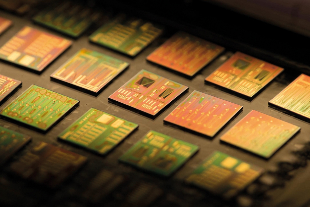
Figure 2: Photonic Integrated Circuit (PIC) under test.
Several JePPIX project partners are already thinking ahead to the next challenges in systems integration. One such example could be the incorporation of micro-transfer printing, which is a method to print active elements such as InP circuits on a wafer-scale by transferring them with a stamp. Using a relatively large area stamp allows simultaneously aligning and bonding multiple devices to a carrier wafer containing passive circuitry like silicon or silicon technology. The current challenge is to enable high-density arrays and functional circuits within the printed stamp, designing for high yield and low assembly variability. To address this and other challenges, the INSPIRE project was created in 2021 with EU funding of €4.9 million to bring transfer printing to a higher maturity level and industrialization. This project, by 2024, aims to achieve TRL 4 and is ideal for applications requiring very low noise lasers, such as fiber sensing or microwave photonics. If successful, it will become the first platform to combine the strengths of InP and SiN photonics and create best-in-class PIC manufacturing. Furthermore, INSPIRE will strengthen the European manufacturing base by developing and implementing processing steps that are key to removing expensive assembly steps in PIC-based product realization. Initially, the methods will be developed for silicon nitride – indium phosphide integration. Later the developed technology can be further ported to silicon CMOS photonics as well, as the optical coupling happens through an intermediate silicon layer. INSPIRE will connect state-of-the-art manufacturing capability to leading-edge applications and industry clusters through JePPIX, ePIXfab, and the EC manufacturing pilot lines.

Figure 3: Schematic representation of the micro-transfer printing process proposed in the INSPIRE project.
In conclusion, the European leadership in foundry technologies for photonic integration is now transitioning to a robust industrial manufacturing capability. The most recent efforts were dedicated to Indium phosphide integration that allows native lasers and modulators to be connected monolithically with a broad range of low-loss devices to simplify assembly and module integration. In perspective it will also provide a route to integration with premium silicon nitride passive components and 8’-inch wafer production on silicon CMOS.
Europe’s flagship PIC pilot line, JePPIX, facilitates the uptake of InP PIC technology in new markets, and with the introduction of micro-transfer printing via the INSPIRE project, there is great promise for greater scalability of PIC technology. Eventually, the combination of performance requirements, market size, and cost requirements will determine what kind of integration technique becomes the preferred technology, and the EU´s pilot line efforts will pave the way for expanding European industry standards for photonic integration.
References
[1] https://www.jeppix.eu/jeppix-pilot-line-in-a-nutshell/


