Loading...
News Article

III-V Epi addresses demand for short lead times

News

Low to medium volume approach shrinks lead-times for MBE and MOCVD, III-V, epitaxial structures, and overgrowth services

Low to medium volume approach shrinks lead-times for MBE and MOCVD, III-V, epitaxial structures, and overgrowth services

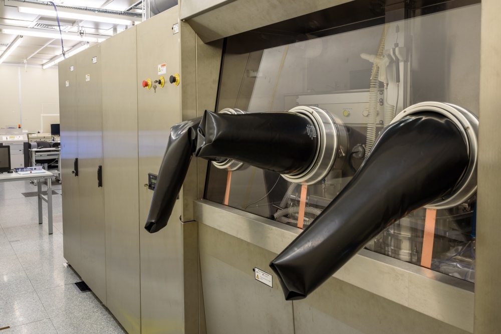
UK-based III-V Epi is providing a fast turnaround service for custom, compound semiconductor wafer design, manufacturing, test, and characterisation.

By focusing on low to medium volume manufacture, the company says it has been able to provide MBE and MOCVD, III-V, epitaxial structures, and overgrowth services with shorter lead times than the industry standard.

Calum McGregor, director of III-V Epi, said: “III-V Epi has helped many customers bring new, compound semiconductor products to market quickly, with its reduced lead time manufacture. This has been achieved by using two key strategies. Firstly, by specialising in medium to low volume supply, we have been able to separate ourselves from the volume part of the industry, dominated by consumer product giants swallowing up the world’s production capacity. Secondly, we have removed potential NPI bottlenecks for customers by offering expertise in every part of the process, from wafer design, product development and process optimisation through to a complete range of test, metrology, and characterisation services.”

III-V Epi says itsunique approach makes it the ideal supply partner for companies requiring low volume supply, such as universities, start-ups, and smaller scale industrial businesses. III-V Epi already supplies devices for communications, telecoms, quantum technology, defence, security, automotive, agriculture and additive manufacturing markets.

Quintessent appoints Bob Nunn chief operating officer
PI to demonstrate new PIC alignment system at Photonics West
Drut launches 2500 product series with CPO for AI datacentres
III-V Epi advocates GaAs for new lasers
Marvell announces new CPO architecture for custom AI accelerators
Printing high-speed modulators on SOI
Photon IP raises €4.75m for advanced PICs
ANELLO Photonics launches Maritime Inertial Navigation System
Aeluma joins AIM Photonics as full industry member
Imec makes breakthrough with GaAs lasers on silicon
POET acquires Super Photonics Xiamen
Voyant Photonics launches affordable Carbon LiDAR
Penn State makes breakthrough in photonic switching
New nanocrystals could lead to more efficient optical computing
QCi awarded NASA contract to apply Dirac-3 photonic optimisation solver
The Netherlands launches ChipNL Competence Centre
TOPTICA to create chip-integrated lasers for quantum PIC project
NSF selects six pilot projects for National Quantum Virtual Laboratory
SiLC Technologies launches Eyeonic Trace Laser Line Scanner
Southwest Advanced Prototyping Hub awarded $21.3 million CHIPS Act funding
Cambridge Graphene Centre and CORNERSTONE to participate in PIXEurope
Cost-effective lasers for extended SWIR applications
IBM unveils co-packaged optics technology for AI and datacentres
QCi announces $50 million concurrent stock offerings
CHIPS Act funding to be awarded to Coherent, Skywater, and X-Fab
ERC consolidator grant awarded for optoacoustic neural network project
Imec demonstrates InP chiplet integration on 300 mm RF silicon interposer
Ayar Labs raises $155 million for optical I/O
Celestial AI awarded 2024 Start-up to Watch by Global Semiconductor Alliance
Researchers develop “last missing piece” of silicon photonics
Quantum sensors for controlling prosthetics
UPVfab to participate in European Commission photonic chips project

×
Search the news archive

To close this popup you can press escape or click the close icon.
Logo
x
Logo
×
Register - Step 1

You may choose to subscribe to the PIC Magazine, the PIC Newsletter, or both. You may also request additional information if required, before submitting your application.


Please subscribe me to:


You chose the industry type of "Other"

Please enter the industry that you work in: