
Hybrid Integration using Electro-Optical Circuit Boards
Hybrid integration methods are gaining attention as PIC
technologies are advancing and requiring sophisticated packaging
solutions. Electro-optical circuit boards, developed by vario-optics ag,
represent a promising platform able to overcome the limitations of
traditional packaging approaches.
By Nikolaus Flöry from vario-optics ag
Photonic integrated circuits (PICs) have tremendously matured over the last decade and found use in a multitude of devices. Photonic chips based on silicon photonic technologies, for example, have expanded their use-case from being employed in transceivers to several other applications, such as photonic computing, optical interconnects and even consumer applications, according to market reports (http://www.yole.fr/Silicon_Photonics_Market_Update_2021.aspx ).
These advancements are not only spurred by extensive research efforts and the addition of new functionalities to the major platforms themselves - silicon-on-insulator (SOI), silicon nitride (SiN) and indium phosphide (InP) - but also by developments on other material platforms and technologies, such as thin film lithium niobate on insulator (LNOI), polymer photonics and plasmonics.
Still, to date, no single platform alone provides all components and functionalities, which are necessary in a typical PIC application such as a complete high-speed transceiver module. SiN exhibits low propagation loss and allows wafer level packaging, but lacks any intrinsic active device functions – such as modulators, photodetectors and most importantly lasers, which is also the major missing building block on the SOI platform. InP on the other hand is an excellent material for integrating laser sources on-chip, but exhibits larger propagation loss and is thus not too suitable for passive devices and large-scale integration.
As a consequence, extensive efforts have been made on developing scalable integration technologies, which allow to leverage the benefits of multiple platforms, combined and tightly packaged together in one module.

Electro-optical circuit board platform based on polymer photonics.
Optical layers containing planar singlemode waveguides are processed
via UV-photolithography and integrated with standard PCB technology. The
EOCB platform provides solutions for (electrical & optical)
PIC-coupling, fan-outs to standard fiber-interfaces as well as on-board
PIC-to-PIC connections.
The importance of integration platforms
The technologies and methods for the combined integration of different PICs can be roughly divided into two branches. One the one hand, additional efforts in the front- and back-end (e.g. micro-transfer printing, direct epitaxial growing) lead to heterogeneously integrated chips. On the other hand, advanced packaging methods such as micro-packaging or on-board co-integration of different chips results in hybrid integrated modules and chiplets.
While the former wafer-scale integration methods hold great promises for low-cost, efficient integration of several chips, the resulting heterogeneous PIC still needs to be packaged – an issue, which has risen in awareness over the last couple of years. As of now, the efficient packaging of PICs still resembles a bottleneck in many applications and has thus become an integral part in any system development involving PICs. This holds true in particular as the complexity of chips is advancing, the number of optical I/Os is increasing and the electrical requirements are getting tighter as well – e.g. high-speed RF interfaces or high-density electrical traces.
In order to overcome the challenges associated with the packaging of PICs, hybrid integration methods are offering significant advantages. They not only allow to combine and connect different PICs together in one module, but at the same time already tackle the issue of packaging, thereby solving two problems at a time. In the following, electro-optical circuit boards (EOCBs) are introduced as an attractive solution to hybrid integration and several technological features relevant for advanced PIC packaging are discussed.

The Horizon 2020 funded QAMeleon project aims on developing novel
scalable transceiver and switches based on a common EOCB platform. a)
InP chips and b) electrical interposer used to mounting on a c) glass
host-board. d) The EOCB integration approach allows to assemble several
chips on one common EOCB, as well as to add micro-optical components
(e). The assembly was performed by Alter UK Technologies
Electro-Optical circuit boards
An EOCB, simply put, is a board featuring both an electric interface (PCB) as well as on-board optical connections (waveguides), which renders it a prime platform for hybrid integration. As for the electrical part, standard PCB technology is used, allowing to include features such as high-speed RF interfaces, (glass) interposers, thermal dissipation layers and vias. Optical on-board connections are created by including polymer or glass based planar waveguides to the board. In the case of polymer, they can be directly manufactured on-board, using the PCB or glass as a substrate. As polymer waveguides have advanced, they can now be operated in singlemode at most common (telecommunication) wavelength and moreover provide solid environmental stability and high power thresholds. Since the dimensions of the cores can be freely adapted and optimized, any passive in-plane device functionality is possible, such as directional couplers or multimode-interference couplers, and as a result of the rectangular cross-section, polymer waveguides are polarization maintaining.
In the case of glass waveguides, the photonic layers can be fabricated separately and laminated with the PCB later on. In both cases, the resulting EOCBs can be designed precisely for the specific requirements of a photonic application, taking into account electrical, optical and thermal considerations, before being equipped with PICs as well as purely electronic components.
The possibility of having one common host board for both the electrical and optical interface is a significant advantage over other integration methods, however often not considered enough. Most PIC packaging efforts only focus on an efficient optical coupling interface. While this is of course a central motivation and requirement in a majority of use-cases, thermomechanical and electrical requirements are often hard to meet this way. The operation of high-power laser chips and high-speed modulators, for example, make it necessary to handle the heat as well as to provide RF above > 100 GHz. EOCBs can handle and fulfill both these needs.
Novel transceiver architectures – QAMeleon project
A perfect example of using this technology for the development of novel transceiver architectures is the Horizon2020 funded project “QAMeleon”. Within this R&D project, novel transceivers and wavelength-selective switch devices are developed, based on InP components and free-space micro-optical elements. The scalability of transceiver and switching technologies plays a key role in the development of future architectures for data-center interconnects (DCIs), as data centers are pushed to their limits due to the ever-increasing demand for bandwidth. Thus, the components developed within QAMeleon are combined and integrated on an EOCB, which is based on a glass substrate featuring metallizations as well as mechanical features for the alignment of the optical and electrical components. Planar polymer waveguides in the top layer of the board are used to couple light in and out of the InP laser and WDM chips. In contrast to bulky fiber-coupling arrangements, the EOCB platform easily allows the scale-up to many parallel optical channels - 18 inputs/outputs (I/Os) - and to match the narrow pitch of the optical I/Os on InP (~30 µm), a key-requirement for multi-port chips.
Glass-Integration into PCB
Apart from its use as an interposer, glass can also be employed as the waveguiding layer itself. Through a process based on ion-exchange, developed by Fraunhofer IZM, gradient index waveguides are created in thin glass. These embedded waveguides exhibit low-loss singlemode operation and can be manufactured on large panel sizes of up to 457 mm x 303 mm.
Together with its partner Varioprint, an advanced PCB manufacturing company, vario-optics has developed a lamination process to integrate such glass panels into electrical PCBs, similar to what has been achieved with polymer waveguides in optical backplanes. The reliability of the glass lamination process is verified by copper metallizations on glass layer, which can be used for conductance measurements after the integration, thus facilitating the process control. Optical interfaces to the glass layer are made by cut-outs in the PCB and CO2 laser cutting of the glass. Laser-structuring of the panels also allows to create trough-glass vias or mechanical features for embedding optoelectronic components. Overall, due to the low propagation loss at telecommunication wavelengths (< 0.1 dB/cm @ 1550 nm), the addition of glass waveguides into large EOCBs is a promising technology for next generation photonic integration.

Glass-based EOCBs. Together with Fraunhofer IZM and Varioprint AG,
vario-optics has developed an integration process to embedd glass
waveguide panels into a PCB.
PIC coupling to EOCBs
One of the biggest challenges in assembling PICs is their typically small mode field diameter in the range of only ~ 1µm. Even though the optical properties of polymer waveguides can be adjusted to achieve small mode fields of down to ~ 4 µm, the remaining mismatch makes it favorable to use spot-size converters on the PIC side as well. Nevertheless, the assembly process of a PIC relying on conventional butt-coupling requires sub-micron precision accuracy. While active alignment processes become easier (and cheaper) over time, this is still a limiting factor in the high-volume production of PIC devices. EOCB offer the additional possibility to include precise mechanical alignment structures (e.g. in glass) on the host board, which can drastically facilitate the assembly process.
Another alternative approach to the assembly is to rely on an adiabatic, evanescent coupling interface. In this coupling scheme, inverse-tapered waveguides on the PIC are used to couple light to exposed polymer waveguide cores, and vice versa. In contrast to grating couplers, this approach provides not only relaxed lateral assembly tolerances (approximately +/- 2 µm), but also efficient coupling over a broad wavelength range for both TE and TM polarization.

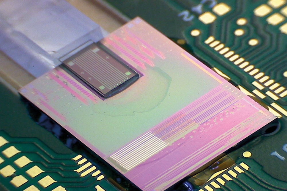
Adiabatic coupling interface on an EOCB. Singlemode polymer
waveguides and electrical bond pads are manufactured close by to allow
simultaneous electrical and optical coupling via a flip-chip bonding
process.
Outlook
As PIC technologies are advancing, the focus is shifting from device-performance only to complete system aspects. Hybrid integration plays a key role in this development, and it is about time that additional efforts are put into the packaging aspects of PIC technologies by academic institutions but also industrial players.
In the end, what is true for the individual PIC platforms themselves also holds for the various integration options: as of now, each approach offers certain benefits and lacks some features, so most probably we will see a combination of them in future applications.
References:
[1] N. Flöry et al., "Highly reliable polymer waveguide platform for multi-port photonic chip-packaging," 2021 IEEE 71st Electronic Components and Technology Conference (ECTC), 2021, pp. 1689-1694, doi: 10.1109/ECTC32696.2021.00267.
[2] C. Zervos et al., "A new generation of high-speed electro-optical transceivers and flexible bandwidth wavelength selective switches for coherent DCI: the QAMeleon project approach," Proc. SPIE 10924, Optical Interconnects XIX, 109240E, 2019; https://doi.org/10.1117/12.2509454
[3] H. Schröder et al., "Low-loss optical single-mode waveguide platform in thin glass with wide spectral range", Proc. SPIE 12007, Optical Interconnects XXII, 120070D, 2022; https://doi.org/10.1117/12.2611775
[4] T. Lamprecht, et al., “Electronic-photonic board as an integration platform for Tb/s multi-chip optical communication.” IET Optoelectronics, 2021, 15: 92-101. https://doi.org/10.1049/ote2.12017


