

Samsung progresses in developing PICs for LiDAR
Microelectronics has truly revolutionized almost every
aspect of life. Efforts to incorporate photonic integrated circuits
(PICs) into advanced CMOS ICs today often center around fulfilling needs
that II-VI or III-V based technologies cannot meet by themselves.
Computing, automotive, wellness and myriad other applications will or
are already benefitting from integrated photonic solutions. LiDAR is at
an inflection point where further advances to reduce size and increase
performance will likely hinge on incorporating new approaches such as
those envisioned by researchers at Samsung’s Advanced Institute of
Technology who report on recent advances in the quest to build a better
PIC for LiDAR.
By: Dongjae Shin, Kyoungho Ha, and Hyuck Choo, Samsung Advanced Institute of Technology
Modern electronics and photonics began around the middle of the 20th century with the inventions of the transistor and laser, respectively. Thanks to the continued evolution of complementary-metal-oxide-semiconductor (CMOS) technology that revolutionized transistors, microelectronics has for decades been a foundation for creating today’s communications and computing systems and countless other innovations [1]. On the other hand, photonics is evolving at a relatively slower pace and is still confined, compared to microelectronics, to diverse but relatively smaller niche fields. Silicon Photonics (SiP) was born under this circumstance. Interest continues to grow as to whether Silicon Photonics can reduce the gap between the two technologies and achieve the commoditization of photonic devices by grafting the productivity of CMOS to photonics [2]. As the CMOS industry has given more technical attention to SiP, it is important to find ‘killer applications’ that can bridge the gap between technologies that can become profitable business opportunities since without a profit potential any technology will not see rapid development. This article introduces recent research by the Samsung Advanced Institute of Technology (SAIT) in support of photonic integrated circuits designed for light detection and ranging (LiDAR) sensors.
Why LiDAR?
In order to explain why LiDAR presents one of the best opportunities for photonic integration among numerous applications, a glimpse into the product development history at Samsung is helpful. One of the most representative missions of Silicon Photonics has been to resolve the DRAM-CPU interconnect bottleneck, the well-known Achilles heel of classical von Neumann computing architectures. Attempts were actively made by Samsung around 2010. Considering the cost limit of DRAM, photonic interconnect feasibility between DRAM and CPU circuits was demonstrated by directly integrating a PIC into a DRAM circuit as shown in Fig. 1(a) [3][4]. Despite such a significant achievement, these attempts also revealed the huge difference in technological maturity between CMOS and photonics, and did not lead to subsequent full-scale development. One of the lessons learned from this experience was that it is very difficult to apply emerging PIC technology directly to legacy applications that have matured for a long time. Samsung therefore concluded that PIC technology is most suitable for emerging applications in many instances.
Among numerous emerging applications considered, LiDAR was chosen for three main reasons. The first reason is its possibility of high volume. Since LiDAR is (or will be) in high demand from various applications such as autonomous vehicles, robots, and smart devices, it is likely to achieve the high volume that can justify CMOS scale production. The second reason is its good timing from the perspective of CMOS evolution as characterized by Moore’s Law and its relentless march towards smaller, faster devices that use less power and cost less to fabricate. Wide deployment of LiDAR has been delayed due to its high cost, so the virtuous cycle of volume and cost reduction from CMOS-like production processes has been an urgent goal for LiDAR development as shown in Fig. 1(b). The third reason is LiDAR’s good match-up with Samsung's PIC platform. While most of the Silicon Photonics industry has been developing PICs on various specialty substrate-based platforms such as SOI, Samsung has developed PICs on a generic substrate-based platform for legacy applications as shown in Fig. 1(c) [5]. Thanks to ~100X higher thermal conductivity of silicon compared to oxide, Samsung’s platform provides better heat dissipation, making it well-suited for heat-sensitive laser or amplifier arrays needed for LiDAR applications. This generic platform, however, is on hold for now, and the specialty platform is used for research purposes. 
Figure 1. (a) PIC embedded in 65nm DRAM. (b) Estimated volume-cost curve for LiDAR. (c) Thermal advantage of generic platform.
Technologies best suited for LiDAR applications
In LiDAR, various technology schemes are competing in terms of performance and cost, and the market winner is still uncertain at this point, especially for low-end applications. The rough consensus about LiDAR architectures is that solid-state solutions are most likely to win rather than mechanical systems with moving parts. Integration rather than assembly of disparate technologies will have an advantage in competition; comparative discussions are actively underway from various viewpoints. The road to an optimized LiDAR solution typically considers three most important viewpoints: planar (XY) illumination, axial (Z) ranging, and wavelength as shown in the Fig. 2. Illumination typically employs the flash scheme, with simultaneous illumination of the entire field of view (FOV) while the scanning scheme employs sequential illumination in each direction comprising the FOV. The flash scheme has already been commercialized for short-range applications by utilizing the existing CMOS ecosystem, and the scanning scheme has been proven for a long time in long-range radio detection and ranging (RADAR) applications. Ranging could involve various approaches such as the time of flight (TOF) scheme that transmits short light pulses while the frequency modulated continuous wave (FMCW) scheme transmits frequency modulated light. Considering that RADAR evolved from TOF to FMCW, it is believed that a similar evolution is likely to occur in LiDAR. In wavelength, there is the silicon-compatible ~900nm band and the III/V-based 1.3~1.5 μm band. The ~900nm band is advantageous from the perspective of the existing industry ecosystem, but the 1.3~1.5 μm band is advantageous from the perspective of eye safety and resistance to ambient light noise. SAIT has been adopting the scanning scheme and the 1.3 μm band with more focus on long-range applications; it is preparing to evolve from TOF to FMCW.

Figure 2. Technology landscapes of LiDAR(a) and RADAR(b).
PICs for LiDAR
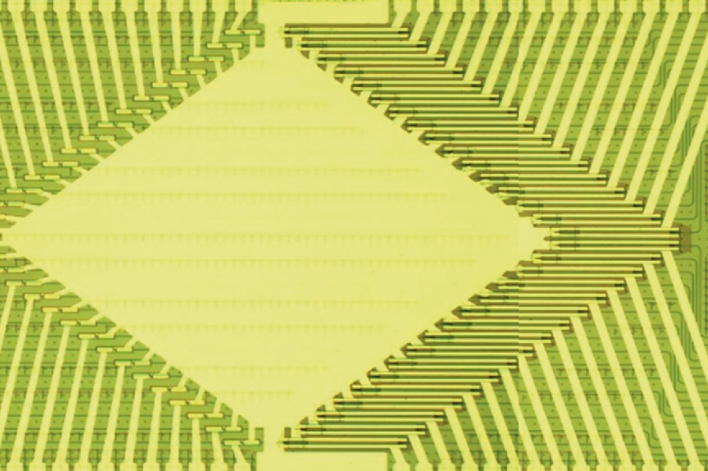
As is appreciated in many photonics applications, to maximize the volume-cost virtuous cycle, it is necessary to integrate all photonic devices on a single chip. Until now, photonic devices for a LiDAR transmitter (Tx) have been integrated into a single chip first, with receiver (Rx) photonic devices integrated after clearing architectural uncertainties. The LiDAR Tx is an optical phased array (OPA) that corresponds to a photonic version of the RF phased antenna array used for RADAR. Figure 3 conceptually illustrates the OPA chip and main photonic devices such as tunable laser diode (TLD), semiconductor optical amplifier (SOA), phase shifter (PS), and antenna array. The OPA amplifies the 32-way split outputs of the TLD by a total of 36 SOAs and controls the phases with 32 phase shifters, thereby reducing the diffusion angle of the optical beam from the antenna array. The optical beam is then scanned by the phase shifters in the horizontal direction and by the TLD in the vertical direction as shown in Fig. 3(d) and (e). The TLD controls the lasing wavelength by the heaters in the two ring resonators shown in Fig. 3(b). When fabricating the OPA, silicon processes were followed by III-V on silicon bonding and III-V processes. This III-V on silicon heterogeneous integration is advantageous for low-cost manufacturing since it simplifies subsequent packaging. The III-V material used for this work is combination of four elements in the group III and V of the periodic table such as Aluminum, Gallium, Indium, and Arsenic, grown on InP substrates.
Figure 3. (a) LiDAR chip integrating TLD, SOA, PS, and antenna array. (b) TLD planar structure. (c) SOA vertical structure. (d) Horizontal beam scan in lower elevation angle with short wavelength. (e) Horizontal beam scan in higher elevation angle with long wavelength.
LiDAR developmental status
In moving toward single-chip integration, the progress of device integration so far is summarized in Fig. 4. From the PoC1 in which only the phase shifter and antenna array were integrated with a silicon-only process, to the PoC2 with additional integration of the SOA, to the PoC3 and the PoC4 groups with additional integration of TLD. These were fabricated through III-V on silicon process [6][7]. From the PoC3 to the PoC4, the circuit layout was improved to reduce on-chip losses and thermal effects [8][9]. The PoC5 with integrated photodiodes (PDs) is also under consideration, but its integration is still ongoing due to delays related to some LiDAR architectural issues. In the PoC1, using a relatively simple silicon-only processes, an OPA with 128 antennas was fabricated, and from the PoC2 with higher III-V on silicon process challenges, OPAs with 32 antennas were fabricated due to lower device yields. The optimal antenna count is determined as part of a performance-cost trade-off, and is expected to vary according to the detection distance required for various applications.
Figure 4. LiDAR device integration progress.
The success of various technology combinations designed to achieve optimal LiDAR performance is summarized in Figure 5. While the PoC1 group had decent resolution with 128 antennas, a very slow frame rate was unavoidable due to low OPA output power and slow external TLD. In the PoC2 testing, because the OPA output power was improved through the SOA integration, video recording at 2 frames per second became possible, but the resolution was lowered due to the decrease in the antenna count. In the PoC3 tests, a 20 frames per second video recording was achieved thanks to the additional integration of TLD, and the resolution was also improved by digital signal processing (DSP) and image signal processing (ISP). In the PoC4 tests, the detection range and FOV were improved as the output power increased by the optical and thermal improvement of the OPA. Efforts to optimize performance are currently underway to reach the performance levels demanded by the market. In particular, improving the FOV is the most urgent variable as indicated in Fig. 5. Since the FOV and range are interrelated, improvements to the FOV should be accompanied by improved range. While a time of flight approach is likely to be sufficient for short-range applications, long-range utility is likely to necessitate using a FMCW approach. Therefore, it is believed that the lower cost of the relatively complex FMCW and the higher performance of the relatively simple TOF would be important to the initial segmentation of the LiDAR market.
Figure 5. LiDAR performance progress.
Future outlooks
In order to anticipate the future technology evolution of LiDAR, it is necessary to look into relevant prior technologies such as those pivotal to the development of RADAR and telecommunications applications. Radar has almost the same purpose as LiDAR, and has undergone technological evolution over 100 years. Telecommunications also uses optical devices and module technology that are common to LiDAR, and has undergone evolution over 50 years. Fig. 6 concisely summarizes the major evolutionary paths of RADAR and Telecom. RADAR started in the early 20th century using a TOF approach, and has evolved into utilizing a FMCW scheme because of the challenges of high-power RF amplifiers. FMCW RADAR influenced the development of telecommunications technologies in the 1970s; interest in a FMCW-like coherent scheme was high. However, due to the emergence of optoelectronic based systems and well-known optical fiber amplifiers, the telecommunications market has been dominated by TOF-like intensity schemes since the 1990s. Beginning in the 2010s when more performance improvement was needed, a coherent scheme was revisited for telecom/datacom applications, and now it coexists with the intensity scheme. One important implication of this evolutionary history is that the amplifier technology has had a significant impact on the evolutionary direction of these devices and timing for development leading to market introduction, which is likely to repeat in the evolution of LiDAR technologies. That is, the timing of the TOF-FMCW transition might be determined according to the degree of success of the SOA-based distributed optical amplification technology as described in this article. Attention is focused on how this technological uncertainty will affect the commercialization of LiDAR technology in the coming years.

Figure 6. Insights from RADAR and Telecom evolution.
Further reading
1. G. E. Moore, "Cramming more components onto integrated circuits," Electronics, 1965.
2. D. Shin, et al., "Commoditizing the uncommoditized: Chip-scale LiDAR," SPIE Photonics West, 2022.
3. D. Shin, et al., "Integration of Si photonics into DRAM process," OFC, 2013.
4. D. Shin, et al., " Bulk-Si platform: born for DRAM, upgraded with on-chip lasers, and transplanted to LiDAR," IEEE J. Lightwave Technol., 2022.
5. D. Shin, et al., "III/V-on-Bulk-Si Technology for Commercially Viable Photonics-Integrated VLSI," VLSI, 2020.
6. C. Shin, et al., “A 10-m LiDAR system using an aperiodic spatially-chirped optical phased array,” CLEO, 2021.
7. H. Byun, et al., "A gain-enhanced silicon-photonic optical phased array with integrated O-band amplifiers for 40-m ranging and 3D scan," CLEO, 2020.
8. J. Lee, et al., “Single-Chip Beam Scanner with Integrated Light Source for Real-Time Light Detection and Ranging,” IEDM, 2020.
9. H. Byun, et al., “Single-Chip Beam Scanner LiDAR module for 20-m imaging,” IEDM, 2021.


