Intel announces hybrid III-V/silicon 8-wavelength DFB laser array

Tightly controlled eight-wavelength laser array on a silicon wafer has matched power and uniform spacing
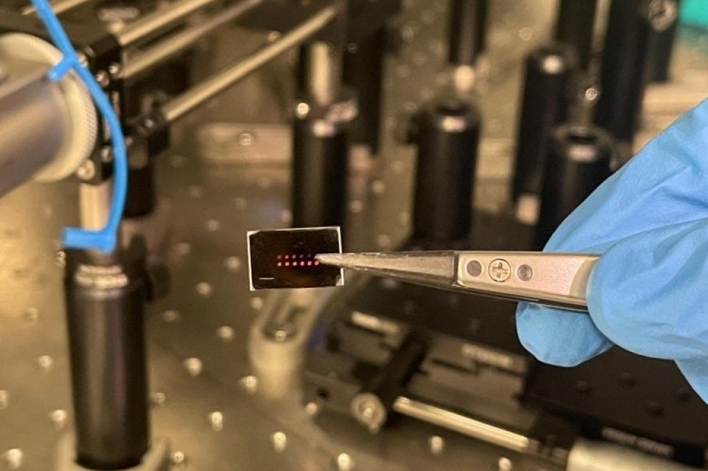
Intel Labs has announced the demonstration of a hybrid III-V/silicon eight-wavelength distributed feedback (DFB) laser array integrated on a silicon wafer. It delivers output power uniformity of +/- 0.25 decibel (dB) and wavelength spacing uniformity of ±6.5 percent that exceed industry specifications.
“This new research demonstrates that it’s possible to achieve well-matched output power with uniform and densely spaced wavelengths. Most importantly, this can be done using existing manufacturing and process controls in Intel’s fabs, thereby ensuring a clear path to volume production of the next-generation co-packaged optics and optical compute interconnect at scale", said Haisheng Rong, senior principal engineer at Intel Labs
Recent co-packaged optics solutions using dense wavelength division multiplexing (DWDM) technology have shown the promise of increasing bandwidth while significantly reducing the physical size of photonic chips. However, it has been very difficult to produce DWDM light sources with uniform wavelength spacing and power until now.
Intel says this new advancement ensures consistent wavelength separation of light sources while maintaining uniform output power, resulting in meeting one of the requirements for optical compute interconnect and DWDM communication. The next generation of compute I/O using optical interconnect can be tailor-made for the extreme demands of tomorrow’s high-bandwidth AI and ML workloads.
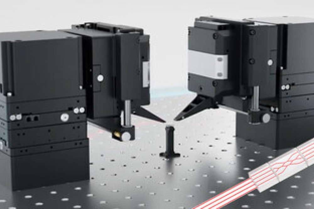
The illustration above shows eight micro-ring modulators and optical waveguide. Each micro-ring modulator is tuned to a specific wavelength. By using multiple wavelengths, each micro-ring can individually modulate the light to enable independent communication.
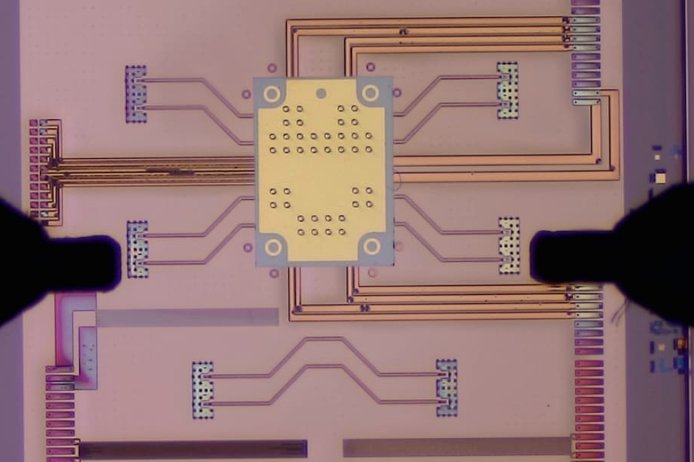
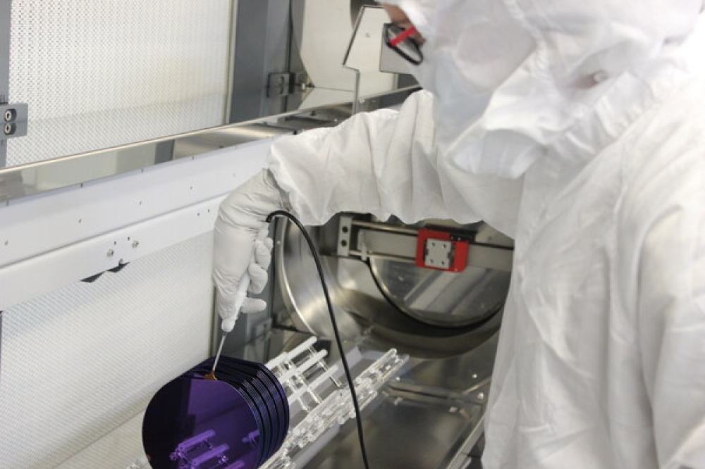
The eight-wavelength DFB array was designed and fabricated using Intel’s commercial 300 mm hybrid silicon photonics platform, which is used to manufacture production optical transceivers in volume.
Intel says this innovation marks a significant advancement in the capabilities of laser manufacturing in a high-volume CMOS fab by utilizing the same lithography technology used to manufacture 300 mm silicon wafers with tight process control.
For this research, Intel used advanced lithography to define the waveguide gratings in silicon prior to the III-V wafer bonding process. This technique resulted in better wavelength uniformity compared to conventional semiconductor lasers manufactured in 3-inch or 4-inch III-V wafer fabs. In addition, due to the tight integration of the lasers, the array also maintains its channel spacing when the ambient temperature is changed.


