
Boosting light power revolutionizes communications
EPFL scientists have built a compact waveguide amplifier by successfully incorporating rare-earth ions into integrated photonic circuits. The device produces record output power compared to commercial fiber amplifiers, a first in the development of integrated photonics over the last decades.
Erbium-doped fiber amplifiers (EDFAs) are devices that can provide gain to the optical signal power in optical fibers, often used in long-distance communication fiber optic cables and fiber-based lasers. Invented in the 1980s, EDFAs are arguably one of the most important inventions, and have profoundly impacted our information society enabling signals to be routed across the Atlantic and replacing electrical repeaters.
What is interesting about erbium ions in optical communications is that they can amplify light in the 1.55 mm wavelength region, which is where silica-based optical fibers have the lowest transmission loss. The unique electronic intra-4-f shell structure of erbium – and rare-earth ions in general – enables long-lived excited states when doped inside host materials such as glass. This provides an ideal gain medium for simultaneous amplification of multiple information-carrying channels, with negligible cross-talk, high temperature stability and low noise figure.
Optical amplification is also used in virtually all laser applications, from fiber sensing and frequency metrology, to industrial applications including laser-machining and LiDAR. Today, optical amplifiers based on rare-earth ions have become the workhorse for optical frequency combs (2005 Nobel Prize in Physics), which are used to create the world’s most precise atomic clocks.
Achieving light amplification with rare-earth ions in photonic integrated circuit can transform integrated photonics. Already in the 1990s, Bell Laboratories were looking into erbium-doped waveguide amplifiers (EDWAs), but ultimately abandoned them because their gain and output power could not match fiber-based amplifiers, while their fabrication doesn’t work with contemporary photonic integration manufacturing techniques.
Even with the recent rise of integrated photonics, renewed efforts on EDWAs have only been able to achieve less than 1 mW output power, which is not enough for many practical applications. The problem here has been high waveguide background loss, high cooperative upconversion – a gain-limiting factor at high erbium concentration, or the long-standing challenge in achieving meter-scale waveguide lengths in compact photonic chips.
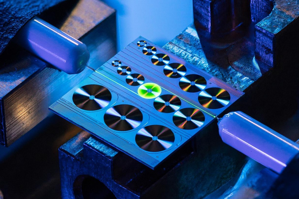
Now, researchers at EPFL, led by Professor Tobias J. Kippenberg, have built an EDWA based on silicon nitride (Si3N4) photonic integrated circuits of a length up to half meter on a millimeter-scale footprint, generating a record output power of more than 145 mW and providing a small-signal net gain above 30 dB, which translates to over 1000-fold amplification in the telecommunication band in continuous operation. This performance matches the commercial, high-end EDFAs, as well as state-of-the-art heterogeneously integrated III-V semiconductor amplifiers in silicon photonics.
“We overcame the longstanding challenge by applying ion implantation – a wafer-scale process that benefits from very low cooperative upconversion even at a very high ion concentration – to the ultralow-loss silicon nitrideintegrated photonic circuits,” says Dr Yang Liu, a researcher in Kippenberg’s lab, and the study’s lead scientist.
“This approach allows us to achieve low loss, high erbium concentration, and a large mode-ion overlap factor in compact waveguides with meter-scale lengths, which have previously remained unsolved for decades,” says Zheru Qiu, a PhD student and co-author of the study.
“Operating with high output power and high gain is not a mere academic achievement; in fact, it is crucial to the practical operation of any amplifier, as it implies that any input signals can reach the power levels that are sufficient for long-distance high-speed data transmission and shot-noise limited detection; it also signals that high-pulse-energy femtosecond-lasers on a chip can finally become possible using this approach,” says Kippenberg.
The breakthrough signals a renaissance of rare-earth ions as viable gain media in integrated photonics, as applications of EDWAs are virtually unlimited, from optical communications and LiDAR for autonomous driving, to quantum sensing and memories for large quantum networks. It is expected to trigger follow-up studies that cover even more rare-earth ions, offering optical gain from the visible up to the mid-infrared part of the spectrum and even higher output power.
Funding
Swiss National Science Foundation (SNSF)
Defense Advanced Research Projects Agency (DARPA)
Air Force Office of Scientific Research (AFOSR)
Horizon 2020


