

Mode-locked comb lasers for chip-scale spectroscopy
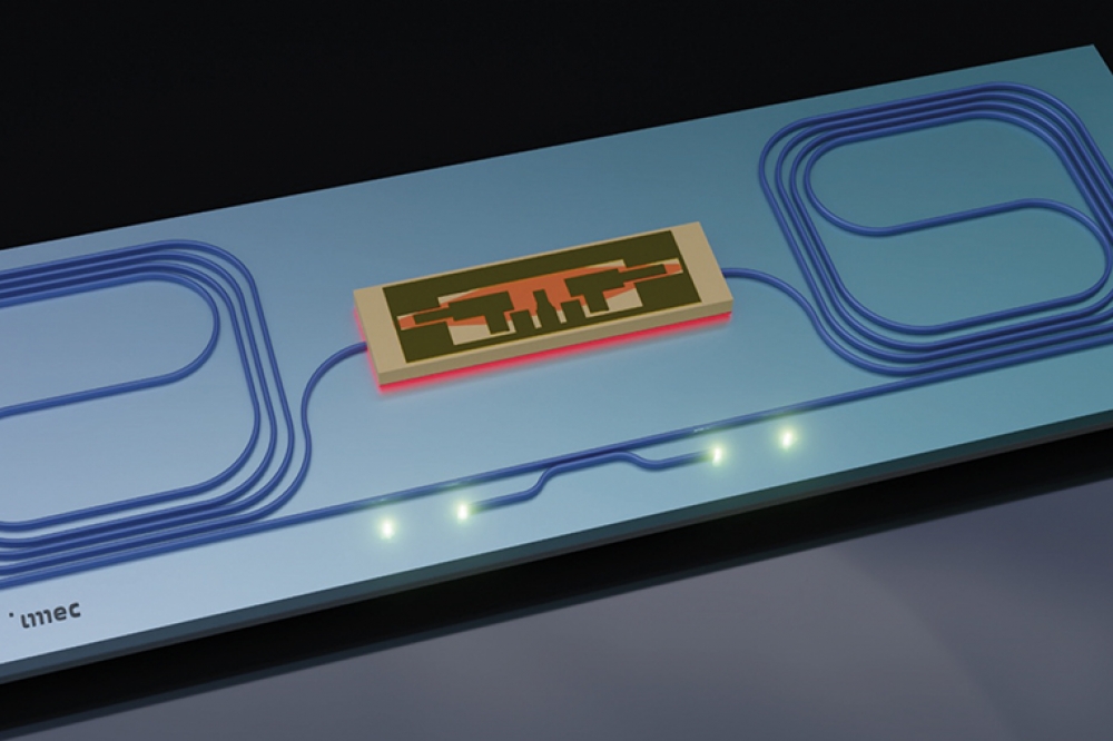
By integrating a semiconductor optical amplifier on a low-loss SiN
photonic chip, an ultra-dense, low-noise laser comb is realized,
delivering unprecedented precision for chip-scale spectroscopy
BY STIJN CUYVERS, BAHAWAL HAQ, GUNTHER ROELKENS, KASPER VAN GASSE AND BART KUYKEN FROM GHENT UNIVERSITY - IMEC
Underpinning a revolution in precision frequency metrology and timekeeping is the optical frequency comb, an optical source that generates a large number of coherent equally spaced discrete laser lines. The impact of these combs has been widely recognized, most notably in 2005, when John Hall and Theodor Hänsch were awarded a Nobel prize in physics for their contributions to the development of laser-based precision spectroscopy, including the optical frequency comb technique.
Traditionally, comb spectra are generated using Ti:sapphire solid-state lasers and erbium- or ytterbium-doped fibre mode-locked lasers. As these laser sources are bulky, their use is restricted to experiments in a lab.
To unlock the full potential of comb spectra technologies, it is essential to develop a compact, mass-manufacturable device. In recent years, considerable effort has been directed towards this goal, with researchers focusing on the integration of optical comb generators on a photonic chip. Success on this front will extend the application range well beyond fundamental frequency metrology to areas such as laser ranging, telecommunications and on-chip spectroscopy.
There has been a great deal of interest in dual-comb spectroscopy, as it allows for a highly multiplexed interrogation of broadband absorption spectra using a single photodetector. This technique enables accurate characterization of rotational-vibrational transitions of numerous gasses, liquids and solids. When using this spectroscopic tool, one comb is sent through the sample under study, while another, with a slightly different line spacing, acts as a ‘local oscillator’. Interfering these two combs on a photodetector generates a frequency comb in the RF domain, composed of distinguishable beats between pairs of optical comb lines. With this approach, the sample’s spectral information is hence readily available in the RF domain and accessible for electronic processing.
One of the merits of this method is that as all spectral components are simultaneously measured, systematic errors, such as temporal variations in the sample, are effectively equalized. Another strength is that the frequency combs can be calibrated with an atomic clock to provide unrivalled precision.
A key requirement for this spectroscopic technique is the ability to generate a dense low-noise optical comb on-chip. As the resolution of the spectral measurement is directly related to the spacing between adjacent comb lines, a denser comb enables identification of otherwise undetectable features in the sample’s spectral response.
Efforts in developing the first chip-scale dual-comb spectrometers employed Kerr-effect combs, consisting of a high-quality optical ring resonator pumped with a continuous-wave laser. Due to the material’s non-linearity, many new frequencies are generated in the resonator, leading to the creation of an optical comb with a line spacing determined by the size of the ring.
There have also been demonstrations involving quantum- and interband- cascade lasers, and so-called electro-optic frequency combs. The latter approach produces an optical comb by placing an electro-optic phase modulator in a resonator with a strong second-order nonlinearity, and pumping it with a continuous-wave laser. Modulation results in the growth of sidebands at the modulation frequency, which are subsequently modulated as well, resulting in a cascading effect.
Although these platforms have shown impressive results, their limited number of usable comb lines, integration challenges and their large comb line spacing (more than 10 GHz), inhibit their use in chip-scale high-resolution spectroscopic applications. In particular molecular spectroscopy in the gas-phase has proven challenging because gasses typically have absorption features with linewidths on the order of 1 GHz. Optical combs with a narrow line spacing are crucial to accurately sample these spectra without the need for interleaving multiple spectra measured at different times.
Fortunately, there is a class of comb generators well-suited to the demands of on-chip gas-phase dual-comb spectroscopy. The breakthrough comes from translating the traditional optical frequency comb technique to a chip-scale device: the integrated mode-locked laser.

Figure 1. Microscope image of the III/V-semiconductor-on-SiN
mode-locked laser chip, consisting of two 10 cm spirals and InP-based
amplifiers and a saturable absorber.
Mode-locked lasers on a photonic chip
Mode-locked lasers are a special class of laser that generate ultra-short optical pulses by phase-locking a large number of longitudinal modes within a cavity. In accordance with the Fourier theorem, such a series of short optical pulses creates an optical comb in the frequency domain.
Engineers can fabricate these devices on a chip using the same manufacturing techniques employed for making continuous-wave laser diodes. The primary difference is the addition of a saturable absorber, which favours the formation of pulses over continuous-wave lasing. Saturable absorbers are typically realized by electrically isolating a part of the gain waveguide and reverse biasing it.
Numerous material platforms have been used to develop integrated mode-locked lasers. They range from InP/InGaAsP and InP/InAlGaAs quantum wells to InAs/InP, InAs/GaAs and InP/InAlGaAs quantum dots. As the noise performance and comb line spacing are proportional to the cavity length, there is a large incentive to extend the laser cavity. This has driven the development of InP and III/V-on-silicon lasers with long passive waveguide cavities.
In 2017, a collaboration between researchers at Ghent University - imec and the University of Eindhoven realised a milestone in integrated mode-locked laser performance. Back then, they unveiled a III/V-semiconductor-on-silicon mode-locked laser with a repetition rate – that is, a comb line spacing – of just 1 GHz. Success came from transferring an InP/InGaAsP gain material, epitaxially grown on its native substrate, on top of a silicon-on-insulator (SOI) passive photonic circuit through a die-to-wafer bonding technique. By combining a long, low-loss silicon waveguide cavity with a high-quality quantum well gain waveguide, this enabled a narrow linewidth and a small comb line spacing.
SiN for ultra-low losses
A promising candidate for propelling performance to a new level is the use of a SiN platform for integrated laser sources. While typical silicon waveguides exhibit losses around 0.7 dB/cm, SiN waveguides can routinely realise losses that are far lower, close to 1 dB/m. Another advantage over their silicon cousins is that, thanks to the higher bandgap, they don’t suffer from nonlinear two-photon and free-carrier absorption that fundamentally limit the attainable cavity size and lasing power.
Our team at the Photonics Research Group of Ghent University – imec has adopted this approach, developing the world’s first on-chip mode-locked laser based on this novel III/V-semiconductor-on-SiN platform. By exploiting ultra-low losses of just 5 dB/m, we have realised the lowest noise reported for a chip-scale mode-locked laser to date and demonstrated a record comb line spacing of a mere 755 MHz, breaking the 1 GHz record.
Our laser has a ring cavity geometry, consisting of two 10 cm SiN spirals, deposited by means of low-pressure CVD on top of a patterned silicon-on-insulator wafer (see Figure 1 for a microscope image of this mode-locked laser). The 330 nm-thick SiN waveguides have been defined using deep-UV lithography, enabling low-cost, high-volume wafer-scale manufacturing.
To enable the heterogeneous integration of a III/V-semiconductor optical amplifier, we locally etch a trench in the 4.2 µm silicon oxide top cladding. This is accomplished with dry etching techniques, and results in a local exposure of the cavity waveguides. Furthermore, we employ a two-stage taper to efficiently couple the light from the SiN waveguide to the III/V gain waveguide. Light first couples from the SiN waveguide to a silicon waveguide underneath, and then into the III/V waveguide. This allows for an improved match in the refractive index and consequently an enhanced coupling efficiency (a microscope image of the coupling structure is shown in Figure 2).
Micro-transfer printing
We use micro-transfer printing for the heterogeneous integration of the III/V amplifier. This process relies on the kinetically controlled adhesion of an elastomeric stamp to pick devices from a source wafer and print them on a target wafer, in this case the SiN Photonic Integrated Circuit (PIC). An overview of the integration process is shown in Figure 3.
An important advantage of micro-transfer printing is its ability to integrate the III/V amplifier in a deep recess, an attribute that is essential for compatibility with low-loss top-cladded passive photonic platforms. Additional strengths of micro-transfer printing technology, which leverages the advantages of flip-chip integration and wafer bonding techniques, are efficient use of expensive III/V material and massively parallel integration, because many devices can be picked up and printed simultaneously. It’s also worth noting that III/V devices can be pre-processed on their native substrate prior to transfer printing, permitting pretesting on the source wafer; and material stacks can be co-integrated on the same target wafer to implement diverse functionalities, offering unmatched versatility.
Fabrication of our devices begins by defining III/V semiconductor optical amplifiers, from here on denoted as ‘coupons’, on the native III/V InP-based substrate. The epilayer stack contains six InAlGaAs quantum wells and is grown on a 500 nm AlInAs release layer that can be selectively etched to release the active region from the substrate. After patterning the coupons, we deposit a photoresist encapsulation, before removing the AlInAs with a FeCl3:H2O solution. This leaves the coupons solely supported by the resist encapsulation and ready for micro-transfer printing.

Figure 2. Microscope image of the micro-transfer printed coupon on top of the two-stage taper coupling structure.
To ensure a high printing yield, we deposit a 50 nm-thick adhesive divinylsiloxane-bis-benzocyclobutene (BCB) layer on the patterned SiN target sample. The source and target are then loaded into the micro-transfer printing tool and carefully aligned. An elastomer stamp picks up a coupon from the source wafer by laminating the stamp against the coupon and then rapidly moving upwards. During this movement, adhesion between the coupon and stamp increases, and encapsulation tethers break at predetermined locations. After this, the coupon-loaded stamp is pressed against the target sample, before it is slowly retracted to leave the coupon behind on the target.
Following the micro-transfer printing process, resist encapsulation is removed and the recess is planarized with BCB. The III/V amplifier is then post-processed, using a series of wet and dry etching steps to electrically isolate a saturable absorber, expose n-contacts and provide electrical contact pads for biasing.

Figure 3. Concept of micro-transfer printing pre-processed
III/V-semiconductor optical amplifiers on a target photonic integrated
circuit using an elastomer stamp.
Record comb density
To evaluate our device’s performance, we have biased the amplifiers and saturable absorber with contact probes and collected the light output with a single-mode fibre. Capturing the optical output with a photodetector allows us to translate the comb spectrum to the RF domain (see Figure 5(a)). This indicates a comb line spacing of 755 MHz, which is, to the best of our knowledge, the lowest reported comb line spacing for an on-chip passively mode-locked laser. Such a low spacing enables an unprecedented resolution for spectroscopic applications. Note that the comb roll-off at high frequencies is not related to the mode-locked laser, but rather a consequence of the 30 GHz bandwidth of the transimpedance amplifier of the photodetector. The optical comb spans over 3.27 nm (see Figure 5(b)), indicating that the laser generates over 500 densely and evenly spaced lines within a 10 dB bandwidth.
Characterisation of the noise properties has involved measuring the optical linewidth of the central lasing mode by heterodyning the output of the mode-locked laser with a tuneable continuous-wave laser on a photodetector (see Figure 5(c)). We fitted the heterodyne signal with a Voigt profile that has a full-width at half-maximum of just 146 kHz. To characterise the repetition frequency signal at 755 MHz, we measured the output of the mode-locked laser with a photodetector and an electrical spectrum analyser (see Figure 5 (d)). The narrow 300 Hz -10 dB RF linewidth indicates that all the optical modes are strongly phase-locked, and implies that the optical linewidth of the comb lines is similar to the linewidth of the central lasing mode. Single-sideband phase noise measurements reveal an amplified-spontaneous-emission-limited RF linewidth of 1 Hz, indicating that the RF linewidth is currently dominated by environmental and technical noise perturbations.

Figure 4. Fabrication process flow. (a)-(d) III/V-semiconductor
optical amplifier fabrication, (e)-(f) micro-transfer printing process,
(g)-(i) post-processing. (a) III/V-epilayer stack, (b) III/V coupon
definition on the source substrate, (c) coupon encapsulation with
photoresist, (d) release etch, (e) pick-up coupon from source, (f) print
coupon on target in recess, (g) encapsulation removal and BCB
planarization, (h) saturable absorber isolation, (i) final
metallization.
Our results showcase the potential of our on-chip mode-locked lasers for integrating high-resolution dual-comb spectrometers on a photonic chip. However, there are still a few challenges to overcome before commercial deployment follows. Firstly, it would be good to have an even larger number of usable comb lines, a goal that could be accomplished by further engineering of the laser cavity and spectral shaping of the gain. Secondly, there is a need to carefully package and stabilize these mode-locked lasers to minimize the impact of environmental perturbations. Another task is to explore other material platforms, such as GaSb, which could target spectral regions beyond 2 µm and enable us to uncover the full capabilities of on-chip spectroscopic sensing.

Figure 5. Experimental results. (a) RF spectrum of the generated pulse
train with a comb line spacing of 755 MHz. (b) Optical spectrum with a
10-dB span of 3.27 nm, measured with a 30 pm resolution. (c) Optical
linewidth, measured by heterodyning the mode-locked laser output with a
tunable laser. (d) Repetition frequency signal at 755 MHz.
The authors would like to acknowledge the Flemish Research Council (FWO) for a Ph.D. scholarship (11F8120N) and a postdoctoral fellowship (12ZB520N). This work was carried out in the context of the European Research Council (ERC) starting grant ELECTRIC.
Further reading
S. Cuyvers et al. European Conference on Optical Communications (2020)
N. Picqué and T.W. Hänsch. Nature Photon 13 146 (2019)
K. Van Gasse et al. arXiv 2006.15113 (2020)
K. Van Gasse et al. IEEE Photon. Technol. Lett. 31 23 1870 (2019)
Z. Wang et al. Light Sci. Appl. 6 e16260 (2017)
B. Haq et al. Laser Photonics Rev. 14 1900364 (2020)


