
Silicon Nitride offers flexibility to move from R&D to volume production
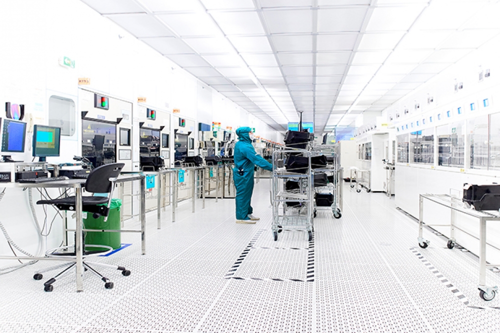
Silicon nitride (SiN) now provides additional pathways to
photonic integration including a new 200 mm, high volume, automotive
qualified CMOS production line. The material platform has gained
maturity over the past years next to well-established silicon photonics
and offers new opportunities in photonic integrated circuit (PIC)
markets for applications that need very low propagation losses, visible
wavelength or high laser power.
Photonic integrated circuits (PICs) are ready to repeat the success story of electronic integrated circuits (ICs). PICs work with light instead of electrons and will play a key role in tomorrow's infrastructure in communication, sensing and transportation. Whereas silicon photonics has been around for more than 20 years, new material platforms have been introduced in the past decade that offer additional benefits.
The motivation for using silicon nitride (SiN) waveguides are manifold. Firstly, silicon nitride is a well-known material that is CMOS compatible and already used in the semiconductor industry. This enabled the development of fabrication techniques and process design kits (PDKs) with standard CMOS tools. This was one of the main requirements when scaling a process afterwards to volume or more importantly when using already existing infrastructure to run the process.
Secondly, silicon nitride as a material offers new possibilities to the PIC market. If we look, for example, at the application wavelength as one major parameter we can see that in classical silicon photonics, where the optical wave is guided in silicon, transparency starts above one micron. This is perfect for many fiber optical applications, especially communications. However, there are many more applications which require light propagation at lower wavelengths that cannot be served by silicon photonics. Silicon nitride with its transparency window spanning from the visible to the mid infrared opens the path for new applications. In addition to that, silicon nitride offers extremely low propagation losses compared to silicon or indium phosphide. Last but not least, high power propagation of several Watts of CW laser power is possible due to the large bandgap of silicon nitride. This is why silicon nitride offers superior performance to manage the light in the chip circuitry with unprecedented low propagation losses and high-power handling.
Existing applications
Telecom and datacom industries are one of the largest PIC consumers as of today. Lowering optical losses is getting more important in those domains, since optical loss affects not only the energy consumption, but also the performance of the devices. The cross-talk performance of arrayed waveguide gratings for wavelength division as MUX and DEMUX for example is directly proportional to optical propagation loss. AWGs with high propagation losses are accumulating phase errors in their arms which results in increased cross talk between the channels. Another key parameter is to have low temperature dependence of the AWG to minimize the thermal effects on device performance. Here silicon nitride offers a 10 times lower temperature dependence than silicon. Additionally, a good process control is needed to ensure the right wavelength band selection. Statistical process control guarantees this with LIGENTEC’s fabrication platform. Especially for AWGs LIGENTEC’s proprietary technology provides a competitive advantage, as not only the loss of the waveguides are very low, but also the area size of the arrayed waveguide grating is small due to the small bending radius common to the platform. This is enabled by the high confinement of the optical mode in the waveguide. The LIGENTEC platform offers very low phase errors together with a small footprint.
New applications
The above-mentioned advantages are also of great importance to other new applications. To enable fully autonomous driving, for instance, it is expected that the next generation of LiDAR sensors for long distance sensing will be based on coherent detection. Here the reflected beam is mixed with a local oscillator, filtering out all light that is not coming back in reflection from the object. These coherent detection schemes are rather complex and benefit significantly from photonic integration. Key requirements for such an FMCW LiDAR system are the ability to transmit high optical power, have low propagation loss and low phase errors and last but not least low cross talk between the transmit and receive channels. A key building block here is the delay line interferometer, used to control the modulation of the laser signal. The length of the delay line is a critical performance parameter since it relates directly to the precision of the range measurement. With the low propagation loss and short bend radius, delay lines of 1m on chip are possible. This in combination with low phase noise enables high resolution FMCW LiDAR solutions.
One of the most promising paths to realize quantum computers is with photons. The only way to achieve a scalable photonic quantum computer is via photonic integration where the quantum states are generated and processed optically. A high phase stability between the individual components is an absolute requirement to preserve the quantum states. The chip technology gives a phase stability which is not achievable with discrete optical components. Moreover, a quantum computer needs hundreds of nodes to be able to compete with classic computers, the components for each node need to be small and scalable at the same time. For all of the above-mentioned reasons, photonic integration is the only way to realize photonic quantum computers. In Quantum Photonics, every photon counts, the biggest challenge is to keep the photon losses at a minimum. A low loss PIC platform is therefore a key requirement for a successful photonic integration.


Xanadu, a leading quantum computation company has recently demonstrated first-time cloud-based quantum computing at room temperature using LIGENTEC silicon nitride chip technology.
To address existing and new applications LIGENTEC has developed a process fabrication offering that goes hand in hand with an extensive process design kit (PDK). The waveguide width is a design parameter and more than 10 process modules are available to create a variety of useful features, e.g. rib waveguides, dual layer waveguides, thermal tuning elements and local cladding openings for sensing applications or heterogeneous integration with other materials.
The PDK library also includes a large range of components and building blocks with known performance and statistical data to be used by designers as blocks to build the circuit. These building blocks range from various kinds of waveguides to splitters, crossings, and delay lines to filters, polarization rotators and polarization filters. Additional building blocks range from mirrors to components for optical in and out coupling. This is supported by design flows with commercial software and design houses with platform expertise.
As silicon nitride is an intrinsic passive material, LIGENTEC has developed special fabrication modules to integrate active materials. With heterogeneous integration, the material of choice can be placed on top of the SiN waveguide. For example, consider a Mach-Zehnder interferometer-based modulator where the optical phase is changed in one arm and the combined resulting output modulated to realize a fast switch or modulator reaching tens of GHz modulation speed. By placing a piece of Lithium Niobate directly on top of the SiN waveguide, part of the light will be travelling in the upper material and can then be manipulated.
The same principle can be applied to bond III-V components such as lasers or detectors.
In September 2021, LIGENTEC announced the implementation of its proprietary, low loss silicon nitride process technology within the X-FAB foundry ecosystem. With this partnership, all essential elements of the PIC ecosystem are now commercially available in volume within Europe, a key requisite to enable the secure and independent supply of the foreseen high volumes in sensors for self-driving cars, quantum computers, biosensors and other applications. Thanks to this strategic partnership with X-FAB, LIGENTEC now takes volume production requests for low loss SiN PICs based on 200mm wafers. In this way LIGENTEC is looking forward to expanding its offering of fast turnaround, high quality, low loss PICs to its existing base as well as new customers.


