New imec research demonstrates fully digital, self-calibrating optical beamformers

Optical beamformers will play pivotal roles in emerging applications targeting assisted and autonomous driving, high resolution earth observation, crop monitoring and 5G communications. Imec’s new on-chip solution is a self-calibrating optical beamformer with no mechanical moving parts, enabling higher resolution performance while being inherently more reliable.
Many new applications (autonomous vehicles, virtual reality, medical imaging) rely on 3D sensors that use the steering, shaping, and focusing of light to visualize the environment. Most current beamforming solutions are expensive and bulky and need to be calibrated and operated by experts. They typically rely on mechanically moving parts to manipulate the sensing light beam, making them vulnerable to defects.
With integrated photonics, it becomes possible to do the beamforming process with a compact photonic integrated circuit. Researchers from the research & innovation hub imec recently published a unique concept for a fully digital, self-calibrating optical beamformer.
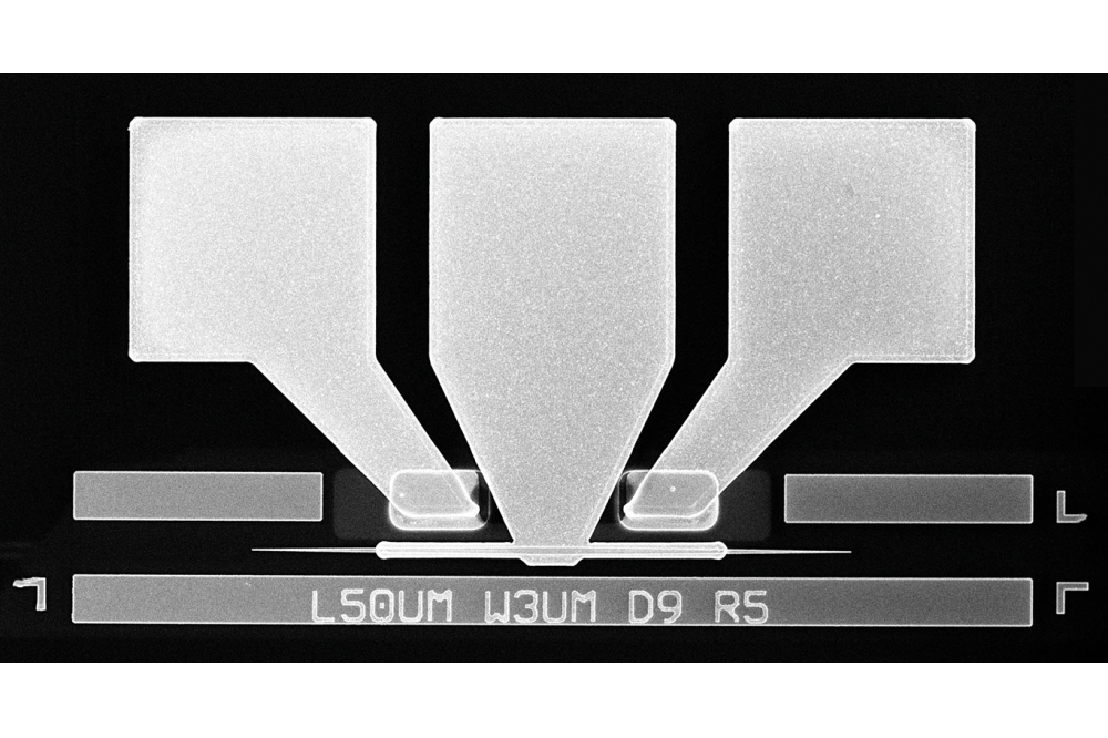
Imec’s beamformer relies on a waveguide that passes through phase shifters to reach an array of on-chip antennas (Figure 1). Through controlled phase modulation, these antennas can transmit signals in a controlled direction.
Figure 1: SEM image of SiN-on-Si optical phase array antenna
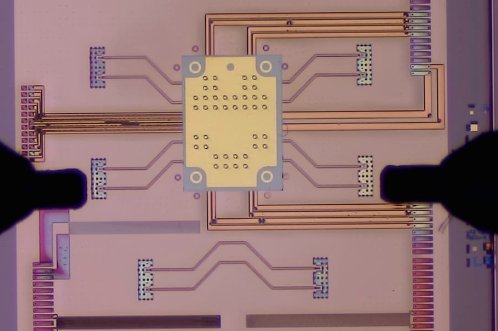
In imec’s latest demonstrators, the beamformer can cover a 40-degree angle (FoV) with below 0.2-degree angular precision. These specifications are not limited by the enabling design (Figure 2) or technology (figure 1) in this demonstration. Actually, it shows that this OPA concept based on Si/SiN photonics is scalable and even tighter specifications could be achieved, based on the customer requirements.
A combination of silicon and silicon nitride
The main novelties of imec’s solution are in the architecture and the choice of material platforms. Where typical solid-state lidar systems are built either in silicon or silicon nitride photonics, imec has made a smart combination of both. Building the waveguide and the antennas in SiN will enable low loss and high-power handling performance plus high process control. In this concept conventional Si photonics is used to build efficient phase shifters and on-chip compact photodetectors. Si-photonics-based phase shifters are the preferred option over the SiN platform to achieve low-power operation and still be low loss.
Because the entire system is compatible with semiconductor manufacturing flows, it allows to drastically reduce the production cost at high volumes using standard CMOS foundry facilities.
Figure 2: Design of the optical beamforming chip fabricated in the imec 200mm photonic pilot line, based on SiN on Si technology for LiDAR application. (From: Kjellman et al. (2020), Silicon photonic phase interrogators for on-chip calibration of optical phased arrays, SPIE conference paper, DOI: 10.1117/12.2546542)
On-chip interferometers for self calibration
On top of its performance and low-cost-manufacturability potential, the imec solution is self-calibrating via an on-chip solution. This is important, because no matter how precise your system is, when processing at the nanometer scale, there will always be slight process and material-related deviations. These result in no antenna or other on-chip building block being 100% identical to its neighbor and inevitably cause deviations in the phase modulation and behavior of the system. As a result, the calibration is required to compensate for these inherent aberrations.
Normally, such calibration is done in a controlled and complex optical setup designed to represent what happens if you would send and retrieve signals over distances of hundreds of meters and to correct for the observed deviations in the measured field. This setup is very unpractical in terms of throughput (when a large number of devices needs calibration) and for use cases where recurring calibration might be needed (e.g. automotive application).
As a solution to this problem, imec has embedded on-chip interferometers in between the phase shifters and very close to the antennas. These assess the actual phase difference between two adjacent antennas. Measured with integrated photodiodes (figure 3), this information provides an absolute indication of the far-field beam quality, (e.g. direction and size,) and allows compensation for non-idealities before the signal gets transmitted.
Figure 3: (left) 2D single-spot scanning-LiDAR demonstration; (right) 2D steerable structured light LiDAR demonstration.
Recently, this technology was used to generate multi-spot sensing by exploiting imec’s design expertise to steer structured-light with a 46-degree field of view in the vertical and horizontal directions (Figure 4).
Figure 4: Cross-section of the silicon PN junction photodiode (From: Dwivedi et al. (2021), All-Silicon Photodetectors for Photonic Integrated Circuit Calibration, IEEE Photonics Technology Letters, vol. 33, no. 16, pp. 836-839, doi: 10.1109/LPT.2021.3065222)
Future work
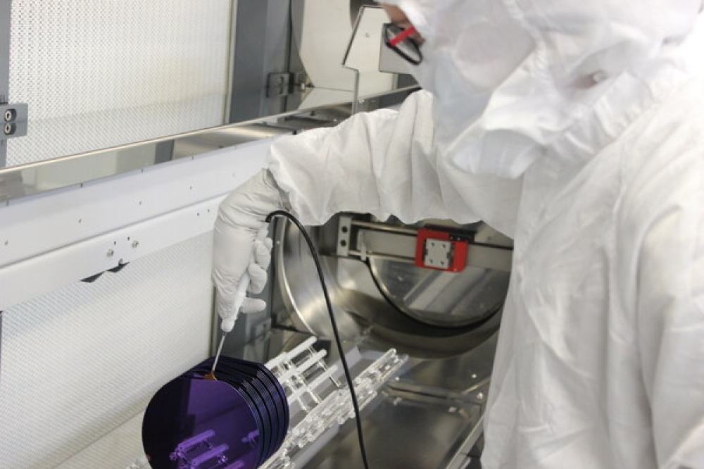
Future work will focus on increasing the beamformer’s accuracy and range. Next, R&D on adjacent components and building blocks that are specific to one or more application domains will be performed. For example, a high-speed linear optical modulator for over air laser communication and microwave 5G applications are part of the imec roadmap. The heart of the research is carried out to allow for device manufacturing in a 200 or 300mm CMOS line using wafer-scale processes (Figure 5) and including electro-optic materials (e.g. BTO) to ensure a lower cost of production. Also, imec will gradually tackle adjacent components such as the photodetectors for signal detection and the ranging engine that does the computation of incoming data.
Figure 5: Wafer-scale PIC manufacturing


