Innovative sensing with integrated photonics
In the last decades, silicon-based photonic has become a key technology for innovative sensing devices because of the growing potential in spectroscopy, process control, emission monitoring, chemical sensing, medical and biological applications.
By CEA LETI
First proposed by Soref in the late eighties, Si – based photonics is now a mature technology covering the full spectral range from visible to Mid-IR and direct access to prototyping and mass production of photonics integrated circuits is now available by many foundries. The availability of PDK tools for fast access to design and fabrication shows that the science and technology of generating, controlling, and detecting light is quickly moving into mainstream electronic designs.
The power of integrated photonics is in the capability to combine on a single chip the reliability and the intrinsic robustness of IC/MEMS technologies with a precise control over wavelength, linewidth, phase pulse duration and power, brought by the heterogeneous integration of the lasers sources directly on Si technological platform.
The main driven for these developments is the strong need for high-performance communications hardware, where photonic ICs is the sole technology offering viable solutions to address technical manufacturability and cost challenges.
However, all major technical achievements designed for Datacom can also profit to other applications, and integrated photonics for optical sensing will be to be a key technology in many field starting from wearable and healthcare applications.
In particular, the developments made for Datacom span out to sensing using Visible or Near IR PICs. In this wavelength region, typically the transduction mechanism used is the modulation of the refractive index induced by local modifications of the environment either by chemical or mechanical stimuli. In chemical sensors, the light can interact with surrounding environment via the evanescent field generated out of the waveguides. However, direct detection in gaseous phase generally gives very low signals, too low to allow reliable measurement. In biological applications, the shifts in refractive index can neither differentiate, nor identify unlabeled analytes due to the complexity of the sample. For this reason, the sensors require an additional process of surface functionalization of the optical device in order to unequivocally identify specific chemicals. As a result, parallel monitoring of multiple analytes need specific functionalization with different receptors (specific polymers, antibodies or markers). The specific receptor interacts with the chemical to be detected, changing the optical properties and the shift of the refractive index can be detected out of the PIC.
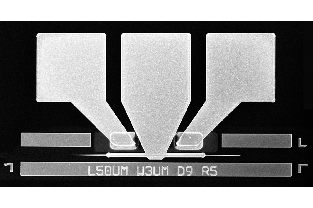
In the case of a mechanical stimulus, the mechanical elements is generally a suspended element, such as a waveguide or a resonant ring, externally actuated at the resonance frequency by an optical force. As presented in Figure 1, the resonant device is coupled via evanescent field to a waveguide at one end and to a mobile beam at the other end. The optical force depends, nonlinearly, on the gap separating the waveguides from the structure and is proportional to the optical power injected in the waveguide. When the mobile beam is set in motion by external physical stimuli – force, pressure, temperature, magnetic field or other – the gap between the beam and the resonator changes modulating the coupling and the variation can be detected out of the waveguides.
Figure 1: Schematics of a optomechanic cavity and example of an optomechanic device made of a resonant ring
The idea of translating and adapting key building blocks to Mid-IR wavelength band was proposed by Soref and co-workers in 2006. Even if many other applications can addressed by Mid-IR technologies, the most mature field of usage is the detection of chemicals in traces either in gaseous, liquid or solid phase. Optical chemical sensing is a fast growing market, driving the technical developments and addressing more and more applications. The main challenge is the co-integration of group IV photonics and III-V heterostructures that allows the development of chemical sensors fully integrated on a single chip. Measuring in the Mid-IR wavelength region, also called fingerprint region, allows addressing a unique combination of fundamental absorption bands order of magnitude stronger than overtone and combination bands in the near IR that can allow high selective, high sensitive unequivocal identification of the chemicals. In fact, a multitude of molecules present strong and distinct absorption lines in the Mid-IR giving much interest for spectroscopic detection.
Spectroscopic sensing in the Mid-IR wavelength band has become commercially available with the advent of unipolar sources based on multiple quantum well stacks. With the recent progress in Quantum Cascade Laser (QCL) and Interband Cascade Laser (ICL) technology, compact and reliable Mid-IR light sources available are nowadays available. In particular, Distributed FeedBack (DFB) sources allow selecting specific emission wavelengths to target the detection of the chemicals of interest. With these sources, a novel generation of sensing tools suitable for real-time in-situ detection of gasses down to traces is nowadays available. In spite of the recent advancements, these tools relying on the assembly of discrete optical components still fail to meet some key requirements required for a large number of applications. In details, DFB sources are weakly tunable (typically few cm-1) and for a large majority of the applications a laser can be used to detect only one chemical. Furthermore, multispecies detection requires a massive use of optics which are intrinsically subject to mechanical and thermal drift. Additionally, the architecture of a typical sensing tool uses of multipass or resonant cavities and cooled IR sensors to measure the relative absorption of the gas mixture: these architectures can be barely miniaturized down to a size compatible with portable applications.
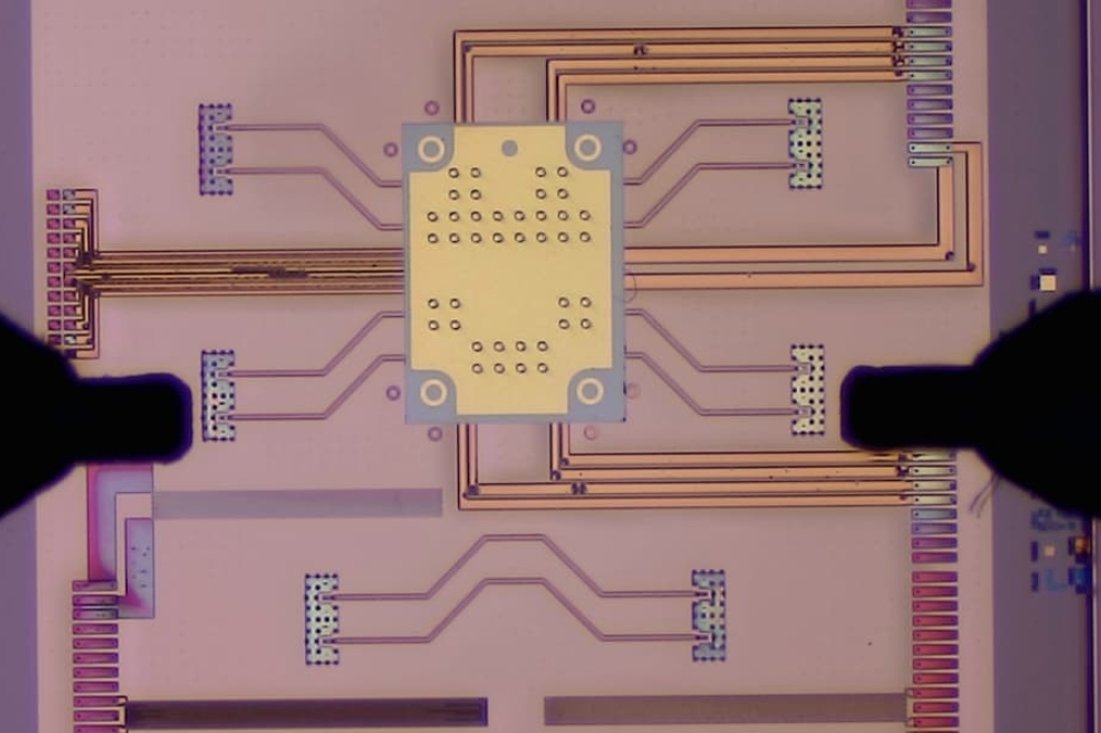
The main focus of the current developments is on i) the extension of the of wavelength range available within a single source, ii) move beam handling and routing from discrete optics to photonics integrated circuits and iii) investigate alternative detection schemes allowing fully integrated on-chip sensing. This approach is presented in Figure 2, where a mockup of a fully integrated optical chemical sensor is shown: an array of QCL sources is coupled to a miniaturized Photoacoustic cell via a PIC circuit allowing combining all the sources in a single output. All the devices are fabricated on Si.
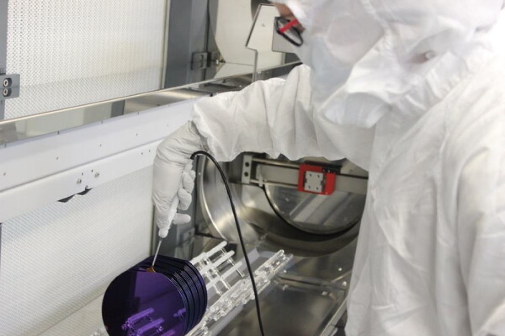
Leti, an institute of CEA-Tech, has been working on these technologies since more than 10 years developing state of the sensors based on photonics devices. Available on CEA-Leti's 200 mm platform in a multi-project-wafer program, these advanced technologies target designers & developers in integrated photonics, LiDAR, chemical and biochemical sensing, and imaging whose projects require chip-level miniaturization and high performance sensing capability.
Figure 2: Array of QCL sources coupled to a miniaturized Photoacoustic cell via a PIC circuit allowing combining all the sources in a single output. All the devices are fabricated on Si on a 200 mm IC/MEMS platform at CEA-Leti.


