Photonic challenges in the next generation of Ethernet

PIC Magazine invited the Ethernet Alliance and EPIC—The European Photonics Industry consortium, to discuss ways that internet access, next-generation photonic integration and the pressures to provide ever-increasing levels of service at lower cost will shape the future of how we communicate, work, and even live. If the pandemic taught us anything of value from a business perspective, it is that we not only can but must be able to run a world remotely. And in a word, to do that we all need: bandwidth.
By: Jim Theodoras (HG Genuine), Ana
Gonzalez (EPIC) & Antonio Raspa (EPIC)
Ethernet continues its relentless march forward, past current 400 Gigabit Ethernet rates, toward the great beyond. As always, a minefield of challenges stands in the way of forward progress, and it will take the combined talents of a global network of technology companies to make it through. The Ethernet Alliance (EA) and the European Photonics Industry Consortium (EPIC) are teaming up to bring industry technology leaders together to make the next generation of Ethernet a reality.
With each new generation of Ethernet, there is more of everything, yet each generation comes with the expectation of lower costs (price, power, form factor or ‘space’) per bit. The conundrum is how to achieve lower costs with ever increasing complexity. There is a hidden cost to complexity, and it is not a linear relationship. The move from one to four channels does not necessarily cost four times as much (4N), but rather can be as much as 42, or 16 times as much. So how to achieve the impossible?
Faster, Wider, Complex
To go faster in optical communications, you can directly go faster (higher bit rate), you can go wider (more lanes of information), or you can increase modulation complexity (increase baud rate). All 3 methods are often employed in unison. The upgrade from 100 to 400 Gigabit Ethernet was a 4X step. On the electrical side, it was accomplished by doubling the bus width from 4 to 8 lanes and doubling the effective bit rate with PAM4 modulation. On the optical side, it was enabled by a 2X step in bit rate and a 2X effective increase in bit rate by moving to PAM4 modulation. Moving beyond 400 Gigabit per second information rates will require at least another 2X step.
Going faster
One option is to simply double bit rates. Existing optical modulation technologies are running out of steam and struggle to meet the nyquist bandwidths that will be required beyond 50 Gbaud per single lane rates. Many EPIC member companies are leading the charge to increase modulator bandwidths involving the use of new materials that can satisfy the new requirements of the industry in the long term. An example is the use of electro-optic polymers to build high-speed modulators that Lightwavelogic develops.
"Electro-optic (EO) polymers can provide much higher speeds and lower power consumption than current semiconductor solutions enabling the very fast switching of light - analogous to what we see when we watch LCD based displays such as televisions, except much faster than the LCD.” Said Michael Lebby - CEO of Lightwave Logic Inc. “These polymer materials have been used to develop a Mach-Zehnder modulators that operate with low drive voltage levels, and speeds of over 100GHz, which represents a 2-3X increase in raw optical device performance over incumbent modulator technologies today. Polymers also have the advantage of being additive and compatible to integrated photonics materials such as silicon photonics and Indium Phosphide, which allows a boost in performance to those platforms.”
On the other side, Polariton Technologies’ electro-optic modulators rely on plasmonics to develop modulators that demonstrated to be more than 10-times faster than current photonic modulators (500 GHz world record in the lab).
“Polariton modulators are >100-times more compact, 10x faster and more energy-efficient than conventional photonic ones,” said Claudia Hössbacher - co-founder and CEO of Polariton Technologies. “Key to our technology is the coupling of light with electrons at a metal surface (Surface Plasmon Polariton, or SPP). In our plasmonic modulators, these strongly confined SPPs interact with an electro-optic material. The tight confinement enables dense integration with device sizes of a few 10s of microns. As devices are small, capacitances are small too, thus boosting the bandwidth. This way, we can keep modulation formats simple and minimize power-hungry DSP.”
Lumiphase enhances the industry-leading silicon photonics platform with Barium Titanate (BTO), a material that allows high speed modulators with >70 GHz, > 10 years life-time in operation and 10x lower optical loss. Transceiver chips based on Lumiphase’s platform are very easy to scale to large volumes in a cost-efficient way.
“Besides the obvious speed benefit, the use of BTO allows extreme low insertion losses which reduces the need for optical amplifiers or powerful lasers while ensuring robust reliability metrics,” Said Lukas Czornomaz, co-founder and Director at Lumiphase. “BTO allows us to address applications in the datacom, telecom, computing and sensing markets, in need of fast, ultra-compact, low-power and cost-efficient light control engines”
Going wider
Another option is to go wider. Just as the jump from 100 Gigabit Ethernet to 400 Gigabit Ethernet included (in one variation) a 2X increase from 4 to 8 electrical lanes, the same can be done on the optical side to quickly realize 800 Gigabit/s information rates. However, this is not without its challenges. Doubling the number of components in the optical system does not necessarily double the difficulty and expense, but rather both may increase exponentially. Current 400 Gigabit Ethernet optical front ends with 4 parallel color channels are at the limits of what can be manufactured using current techniques of combining discrete components on optical benches. Market pressures are driving costs per bit of optical information transmitted down, and anything beyond 400 Gigabit Ethernet will need to cost less per bit, not more.
Increasingly, the industry is realizing anything beyond 400 Gigabit Ethernet will require at least some level of wafer level integration of photonic elements – also sometimes referred to as Photonic Integrated Circuits (PICs). These can be as simple as 4 modulators on a common silicon bench or as complex as an entire coherent optical front end on an InP wafer.
An example of increasing capacity through PICs is The PASSION transmitter basic module that integrates 40 VCSELs and 100-GHz spacing multiplexers in a single Si photonic chip, using massive photonic integration to achieve up to 2 Tbit/s capacity per module. This module is the basis for developing an innovative sliceable bandwidth/bitrate variable transceiver (S-BVT) based on a modular approach to enable multi terabit transmission, providing an important reduction in terms of cost and power consumption. PASSION employs low-cost energy-efficient light sources — namely single-mode InP VCSELs from Germany-based VERTILAS — that operate in the C-band. These sources have a high modulation bandwidth (around 20 GHz) and are directly modulated using PAM-4 or other multicarrier modulation formats, such as DMT, allowing at least 50 Gbit/s capacity per VCSEL. Four modules can be tuned by temperature, in a range from 0 to 75 GHz and interleaved with a spacing of 25 GHz, to obtain a 160-DWDM channel supermodule with a total capacity up to 8 Tbit/s.
In addition, by exploiting polarization division multiplexing (PDM) and combining two identical supermodules that are orthogonal in polarization, a capacity of 16 Tbit/s can be achieved. Furthermore, space division multiplexing using multicore fibers or bundles of fibers enables the achievement of more than 100 Tbit/s per link.
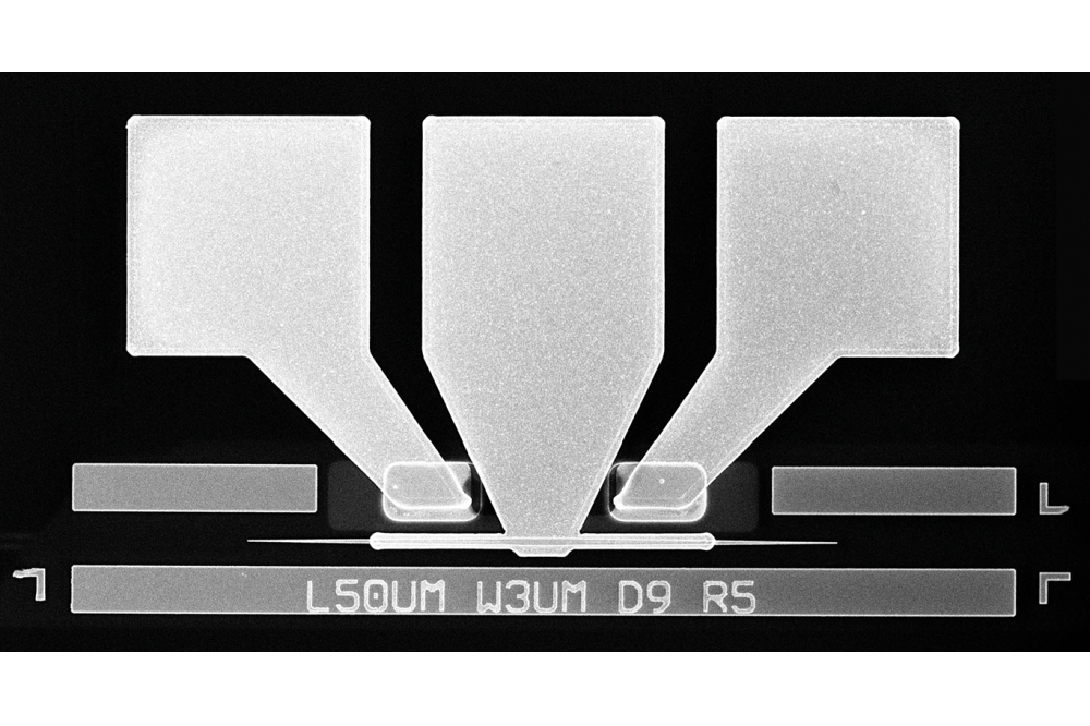
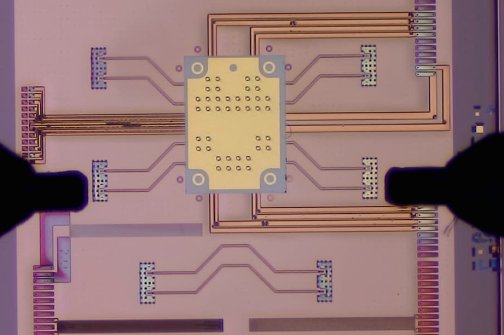
However, when talking about monolithic integration, InP technologies are set to drive a revolution in cost optimization for the next generation of coherent networks. An example of this technology is the Netherlands-based EFFECT Photonics which has developed the world’s first fully integrated coherent PIC targeted at pluggable coherent transceivers for edge and metro/access networks which fits into the smallest modules (Fig. 1): QSFP28 and QSFP-DD. Main applications are multi-rate coherent 100-600G and low power short-range mode (10-200 km) and high OSNR (2000-8000) modes.
Fig. 1 Fully integrated coherent PIC fabricate by EFFECT Photonics (courtesy of EFFECT Photonics)
“Monolithic integration allows for the integration all functionalities such as lasers, modulators, detectors, splitters, and network filters, monolithically integrated in a single chip,” Said Tim Koene CTO at EFFECT Photonics. “This technology allows scaling volume production for applications such as metro-access and datacenter.”
The challenge of PICs
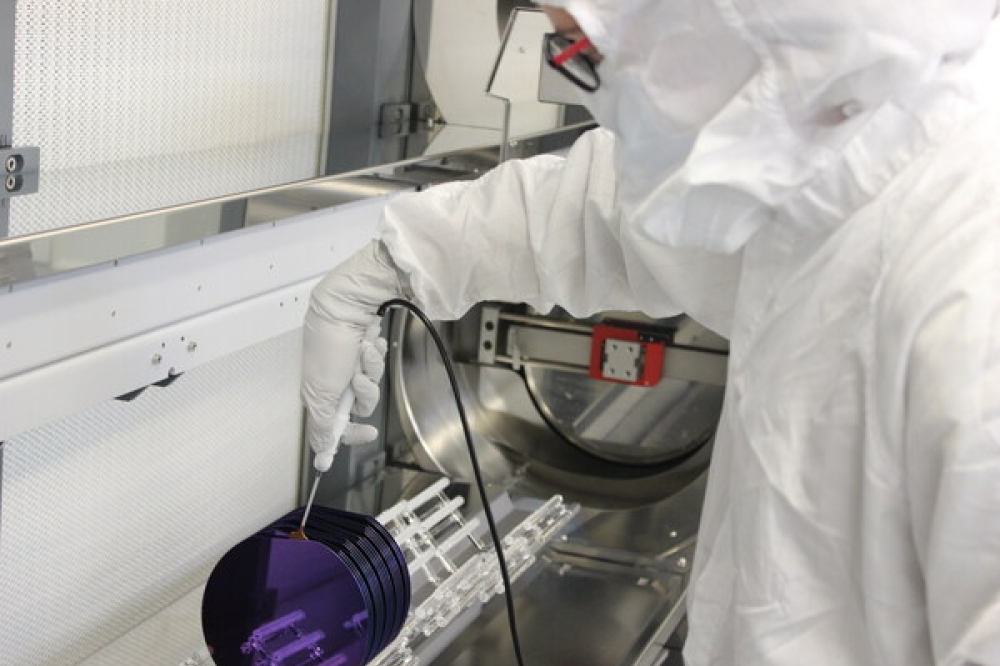
While as scientists and engineers, we like to focus on the physics of how to create and integrate optical functions on semiconductor wafers of various types, the real-world challenge of PICs is how to test them. With discrete optical components, you can test laser power, back-reflection tolerance, color combiner/splitter passbands, modulator Vpi and bandwidth, photodiode responsivity, etc. by simply connecting a tester to each. However, once one or more of these functions is integrated onto a wafer, testing a parameter becomes much more difficult. And waiting until the PIC is integrated into a final product to perform functional validation is not economically viable. Poor performing optical elements need to be caught early in the production process, most often even before the whole wafer is cleaved into individual PICs.
Many EPIC member companies specialize in wafer-level testing of PICs. Wafer level testing is more than buying a unique test machine. Testing strategies must be chosen early in the PIC design process and test features incorporated. EPIC companies are trusted advisors that can work with you early in your PIC design to make sure you are ready for wafer-level test day one.
Companies developing high-precision automation tools such as Ficontec, Aifotec, Tegema and IMS-NL are working together with companies developing testing tools such as Roodmicrotec, Exfo and Quantify photonics, for developing wafer-level testing. Companies such as Photonics42 have developed custom-made and proprietary tool capabilities for wafer level testing: probe cards, instrumentation and measurement system design, modular and multi-channel probing, automation software.
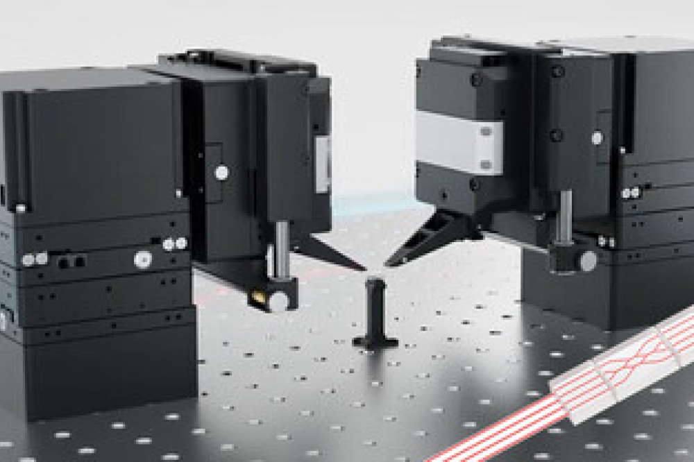
Jenoptik’s new UFO Probe™ technology targets the market for semiconductor equipment and processes for wafer-level testing in microelectronics. The technology is based on a concept for optical probing of photonic integrated circuits, which is insensitive to alignment tolerances in the wafer prober. As consequence, the opto-electronic probe card can be used with commercially available wafer probers and ensures an accordingly high throughput for testing photonic integrated circuits.
Automated manufacturing and alignment
With the increasing number of optical channels and the move to PICs comes an additional challenge – the time and cost of precise alignments, both electrical and optical. Most electrical circuitry is still kept off of PIC substrates. Instead, they are located along the edges or underneath the PIC. Both require very precise alignments, whether for bond wires or bump bonds.
Optical alignments are very challenging with PICs. A single optical alignment can quickly eat into cost, time, and power budgets as two elements have to be aligned within 6 degrees of freedom. With PICs, there can be dozens of alignments to be performed. PICs currently come in two main categories, those with integrated lasers and those with external lasers coupled into the wafer. Both eventually need to couple the output into parallel optical ribbon fiber.
Companies such as Ficontec and ASM AMICRA develops machine providing high-precision die bonder/flip chip bonder which supports ± 0.3µm @ 3s placement accuracy. A side effect of the increasing number of optical channels and alignments to perform is laser powers are increasing. To compensate for the additional coupling and waveguide losses, PIC designers are simply increasing their source laser power. However, this is a self-defeating strategy as issues typically seen with lasers only increase the harder you drive them. And coupling losses can quickly outpace laser drive. The better solution is to simply tackle coupling losses directly.
Several EPIC member companies have novel ways of improving the coupling of light on and off wafer and PIC structures such as Vanguard Automation, which offers machines and processes for automated multi-chip packaging based on 3D nano-print technology (Fig 2.), creating low-loss connections while lowering overall packaging cost.
Fig 2. Photonic integration with 3D-printed lenses fabricated on wafer level (courtesy of Vanguard Automation).
a Schematics of the concept: After drop-casting of liquid photoresist, a lithography tool localizes all components with sub-100-nm-precision on wafer level. The lithography tool solidifies resist by scanning within a pre-programmed lens shape. After lens fabrication, an automated processing tool develops the lens.
b 3D-printed lenses allow relaxing alignment tolerances in a beam expansion approach and facilitate optical assembly.
c Electron microscopy (SEM) image of a chip-facet-attached lens.
Multiphoton Optics offers 3D Direct laser writing equipment that works using two-photon polymerization, a maskless direct laser writing technology. Nanoscribe also offers Two-Photon Grayscale Lithography system is designed for ultra-smooth micro optics with excellent shape accuracy in just one fabrication step and with enormous design freedom.
Guaranteeing reliability
The move beyond 400 Gigabit Ethernet to whatever is next comes with a substantial leap in complexity. Whether discrete or integrated, optical bench or PIC, silicon or InP, all potential solutions will be more complex than ever before. The only way to guarantee reliable operation of such complex optical systems is burn-in. And like performance testing, the earlier you burn-in a product in its manufacturing process, the better.
Integration techniques have the potential to make early burn-in of optical devices difficult if not impossible. Ideally, burn-in of anything with wafer level integration should occur at the wafer level. And like with performance testing, wafer level burn-in requires a strategy day one with supporting features included in the design.
EPIC has several member companies with expertise in how to plan and execute wafer level burn-in of integrated optical devices and PICs such as Yelo and Aehr dedicated to developing test and measurement equipment.
Conclusion
Each new Ethernet speed step begins with exasperation, as veterans of the previous generation ponder how hard it was to reach the current level, their bag of tricks emptied by the effort. But as we as an industry embark on this latest endeavor, if we work together and bring all our technology to bare on the problem at hand, the next generation of Ethernet will become reality. The Ethernet Alliance and EPIC are proud to be a part of bringing together like-minded companies to work on the challenges ahead.
Acknowledgment:
PASSION is a research and innovation actions project funded by the EU’s HORIZON 2020 and develops innovative photonic devices and an optical fibre network infrastructure for a sustainable metropolitan network in terms of huge capacity, low cost, reduced footprint, and low power consumption. PASSION technology exploits the capabilities of VCSELs by developing 25-GHz-spaced InP C-band WDM single-mode VCSELs directly modulated to achieve up to 50 Gb/s per SOP (state of polarization). Multiple single-mode VCSEL modules on silicon-on-insulator (SOI) chips adaptively load/manipulate the spectrum at the subwavelength level to generate flows aggregated to enable up to 16 Tb/s capacity per channel. This project has received funding from the European Union’s Horizon 2020 Research and Innovation Programme under grant agreement No 780326 and it is an initiative of the Photonics Public Private Partnership.
This content reflects only the authors’ view and the European Commission and Photonics 21 are not responsible for any use that may be made of the information it contains.


