
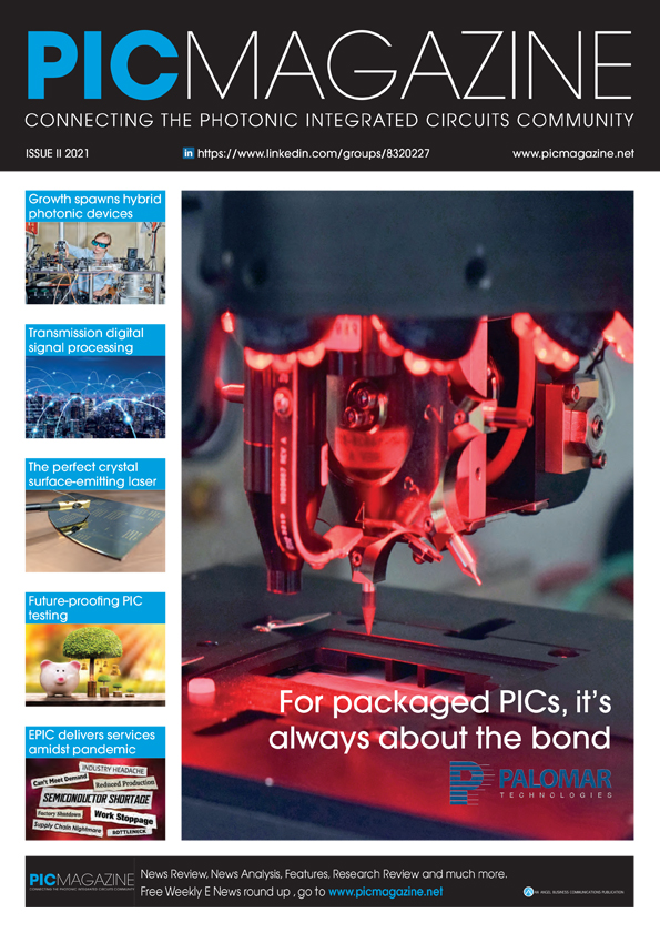
For packaged PICs, it’s always about the bond
Silicon photonic (SiP) devices and photonic integrated
circuits (PICs) are revolutionizing telecom/datacom markets. The growing
capabilities of PICs have also spawned new approaches to advanced
computing and myriad new market opportunities that legacy technologies
cannot address.
PIC Magazine spoke with the experts at Palomar
Technologies to learn how die bonding continues to evolve and play a
central role in SiP and PIC manufacturing.
The universality of some semiconductor processes points to their essential nature across technological platforms. Even as device form factors, lithographic innovations and defect management techniques come and go, there remain some steps that are always needed including the requirement to place finished die inside a receptacle that will protect it and enable its functionality.
While semiconductor manufacturing across technologies is considered the most complex of any industry, the potential for ICs to transform every major aspect of the human experience drove innovation like little else in the last 50 years. Today’s devices are quite literally orders of magnitude better than previous generations; even as per unit costs shrank, performance has soared. PIC and SiP devices are now entering the growth ramp that microelectronic devices faced decades ago. Like their microelectronic counterparts, PICs today face growing pains to automate and address unique testing requirements.
Much as we have seen within silicon logic and memory device manufacturing, PIC producers are keenly aware of the need to finely tune process steps and material formulations to aid in defect elimination and quality control. The test and measurement sector of PIC and SiP manufacturing has also stepped up with ways to automate and improve product quality, reliability and repeatability. These advances help reassure end users than a PIC device can be as reliable as any commercial microelectronic IC.

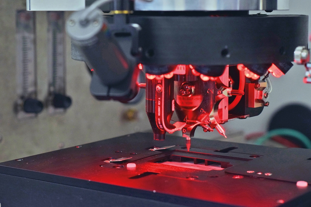
Die bonding is a prime example of how a technology that has been a part of semiconductor production predating automation has continued to evolve and bring value to complex systems including PIC manufacturing. In a recent conversation with Palomar Technologies’ Kyle Schaefer, product marketing manager, PIC Magazine technical editor Mark Andrews spoke about ways that die bonding has evolved, and how advances in the field can contribute to balancing the need for high throughput with process control. PICs of all types are traversing the sometimes perilous path between R&D, low rate production and high volume manufacturing.
Because PICs and SiP devices are still maturing technologies, many manufacturers are also relatively new, seeking efficient means to transition from R&D or proof of concept into production. Given the different developmental stages that PIC manufacturers find themselves, almost all need an economical means to transition from one stage to another. Having process tools that work in R&D as well as in production is an astute investment strategy, a fact that Schaefer says characterizes most Palomar Technologies customers.
One such customer is Bay Photonics that operates out of the Epic Centre, a business incubator serving the counties of Devon and Somerset in South West England, UK. The Epic Centre is part of the Torbay Development Agency that encourages and fosters new business ventures and manufacturing within the region. While not all companies operating out of the Epic Centre are developing photonic devices, many are, and according to Epic Centre Director Wayne Loschi, purchasing the Palomar Technologies 3880 Die Bonder was a decision made after 13 months of various tenant companies using the bonder for many wide-ranging requirements. The purchase was a ‘natural’ decision after administrators saw how many companies were utilizing the tool at many different levels of product development.
Schaefer said one Bay Photonics staffer who truly put the bonder through its paces was John Coombes, senior process & development engineer. Coombes’ company moved into the Epic Centre to further develop their capabilities as a PIC assembly and packaging house. The company’s objective is to reduce their customer’s investment in the direct costs of packaging and assembly for proof of concept devices, prototypes, pre-production devices and production PICs.
“With Bay Photonics recent move to Epic we have challenged the Palomar 3880 on-site here with a range of devices requiring exploitation of its multiple process capabilities, from epoxy dispense to daubing of glass paste and attachment of multiple piece parts to create a photonic subassembly. Bay Photonics – working with Palomar on the Palomar 3880 Die Bonder – has shown that it is a great working platform with good flexibility for handling innovative Photonics enquiries,” Coombes said.
“It has allowed Bay to present bumped PICs and place them with good accuracy onto a tile with specific pad locations and attach with thermosonic and eutectic attachment methods using sinter materials to investigate potential methods and materials.”
“The die bonder consistently demonstrated its powerful programming, high level of tooling process control and intelligent pattern recognition capability from dispensing to picking and placing of die and SMD components though to accurate offset placement of glass blocks attached using the Palomar controlled eutectic nest in a specific position. Furthermore, the flexibility offered with its processing capabilities and tooling array has given Bay confidence in the machine’s capabilities; it offers a great platform for innovation,” Coombes concluded.

Schaefer said that he found Coombes’ remarks about the Palomar 3880 Die Bonder to echo similar comments from other customers regardless of whether they worked in PICs or microelectronics. Features like the 8-tool bond head offer benefits that any production or R&D environment could appreciate.
“Flexibility is key to providing a strong ROI across many business models from academia, SME’s, CM’s, to full scale manufacturing giants like Lumentum & II-VI. Typically, Palomar customers keep Palomar bonders for many years, so longevity of support and the ease of reconfiguration as products and processes mature and change is a major consideration for engineers and procurement professionals when investing in bonding solutions.”
“Specifically, flexibility is one of the core design philosophies of the Palomar 3880. The flexibility of the system is unique in that it offers the capability to easily change from one process or configuration to another while also remaining effective in its performance for all potential applications.”
“It is not just the 8-position, bi-directional tool turret, which only takes 250ms to change tools on the fly, that makes the 3880 extremely flexible. It is the extra-large work envelope where many configurations of bonding hardware, material presentation options and automation options can be utilized. In addition, the changeover is rapid and effortless, which supports any company’s need for high mix.”
“Essentially, the robust abilities of the software and hardware are the core functionality that make the flexibility of the 3880 so impactful, in that it is not just great in one area and good in many others, but it is great in all areas. The 3880 is an R&D, NPI and volume production machine all in one,” Schaefer stated.
While flexibility is a key asset for any tool, some tools that tout flexibility are somewhat more targeted towards R&D or academia where dozens if not hundreds of individuals might use the equipment over its lifetime. Schaefer explained why the value of the Palomar 3880 Die Bonder is wide reaching.
“The 3880 is very popular with research institutes, but equally popular with companies that are churning out high volume transceivers or complex multi-chip modules (e.g. aerospace and defense.) Contract manufactures who are running high mix or medium volumes also love the flexibility of the 3880.”
“It is very common to sell systems to research institutes, but just as common to sell to those customers with a wide range of bonding requirements. However, one of the primary selling reasons relating to its flexibility is the idea of a long-term solution for the customer.”
“Specifically, the 3880 Die Bonder is attractive for its ability to evolve and adapt to a customer's constantly changing process and/or product requirements. Customers heavily value the ‘future-proofing’ concept that the 3880 brings. Even if they make a complete switch to a different product with a new process, the 3880 can and will support that product’s prototyping, development and eventual full-scale manufacturing.”
“Although the majority of 3880 customers do not have a wide range of die bonding requirements at the time of purchase, many can see the possibilities of needing those various capabilities at some point in the next several years. These customers tend to fall within the telecom and datacom markets,” Schaefer remarked.
The PIC / SiP product development and manufacturing ecosystem is evolving rapidly. While datacom and telecom photonic applications are being actively explored, many other applications are just now being considered while others are moving into early prototyping. A natural question arises given this history: for new companies, is a Palomar Technologies 3880 Die Bonder the right investment?
“With nearly 50 years of experience in semiconductors and photonics, Palomar has a history of developing solutions for new market applications. The company is active in the 5G roll out, 3D Sensing and LiDAR, quantum, IoT and AI, VCSEL and PD applications to name a few. There are definitely huge opportunities in quantum device assembly.”
“The 3880 is ideally suited for any development of future applications and opportunities presented in PIC or the photonics market. It is considered the most flexible, balanced die bonder on the market. Because of this and its many capabilities, it is well suited for aiding companies to break into new markets. The 3880’s ability to rapidly change configurations greatly aids in prototyping and proof of concept, which makes it both ideally suited for development of new markets, but should the market come to fruition, it is also ideally suited for production.”
“The wide range of eutectic, epoxy, flip-chip, thermocompression, UV curing and atmospheric plasma cleaning capabilities make the 3880 the only die bonder which future proofs the investment in the system and gives PIC developers the tools and processes needed in the future to further develop exciting new disruptive PIC technology applications.”
“The 3880 is a single piece of equipment that can be configured to handle a high-mix of applications and processes with minimal changeover/setup time, so previous production and new process developments or productions can be run ‘back-to-back.’ The Palomar 3880 is the product of 30+ years of accumulated die attach knowledge and continual improvements in hardware and software to better meet the needs of current and future manufacturing challenges,” Schaefer concluded.
As PIC and SiP processes and manufacturing goals change along with succeeding device generations, some needs remain constant, like the requirement to pick and place die while creating a permanent, robust bond between the device and its package. The Palomar 3880 remains a centerpiece of both research and all manner of production environments. Sometimes, the best products just keep getting better.


