PI’s Fast Alignment Testing Technology Adds Benefits of ACS Controls
Fast, accurate and repeatable testing requirements have in
the past impeded the rapid roll-out of photonic integrated circuits
(PICs) and related components at cost-effective, high volume scale.
Physik Instrumente has pioneered fast optimization technology and has
added new algorithms and alignment-enabled controls from ACS to achieve
productivity gains for large-format optic and photonic production
processes.
By Scott Jordan, Head of Photonics; Senior Director, NanoAutomation; PI Fellow PI (Physik Instrumente)
Physik Instrumente's (PI’s) fast optimization technology has proven to dramatically improve production economics in processes as diverse as photonics wafer probing, device packaging, and chip testing and even laser and optical equipment manufacturing. The combination of speed, nanoscale performance and industrial robustness is reducing costs and improving yield worldwide.
Now the flexible combination of PI´s industrial stages and new alignment-enabled controls from ACS address additional tough throughput and yield challenges for photonics production. Large-format production processes can now be addressed, with each mechanism contributing intelligent alignment for test and assembly. This opens new possibilities for hyper-efficient systems architectures.
PI’s unique optimization functionality is firmware-based, offers the unique option of parallel alignment across multiple inputs, outputs and degrees-of-freedom, and can improve process throughput by a factor of 100 or more compared to legacy approaches.
Background
Alignment automation emerged three decades ago. In an era dominated by single-mode pigtailing applications, it was an enabler that helped eliminate costly manual submicron-alignment processes during device test and assembly.
The photonics world has advanced, though. Wafer-based photonics now drives the industry. Adoption volumes are orders of magnitude higher than in the 1997-2001 photonics boom, and the devices are quite different. For example, multiple I/Os necessitating multiple degree-of-freedom optimization, with each coupling frequently presenting non-Gaussian multimode cross-sections and interactions across channels, inputs and outputs, and DoFs. While these challenges can often be met with legacy alignment techniques, the minutes-scale times required present serious challenges for production economics.
PI’s unique, fifth-generation optimization technology, now well-proven in the field after its 2016 introduction, allows simultaneous alignment across channels, I/Os and DoFs, even when they interact due to optical or geometric crosstalk. The throughput improvement of this parallelism can often exceed a factor of 100, as PI routinely demonstrates in live demonstrations at conferences. So, for example, an array-device alignment that previously took a few minutes can often now be achieved in a second or less.
PI’s first implementations of this technology were in fast piezo stages and hexapods. Now its key functionality has been extended to ACS controls, bringing the benefits of ground-breaking productivity to large-format applications as diverse as photonics wafer probing, device packaging, and chip testing and even laser and optical equipment manufacturing.
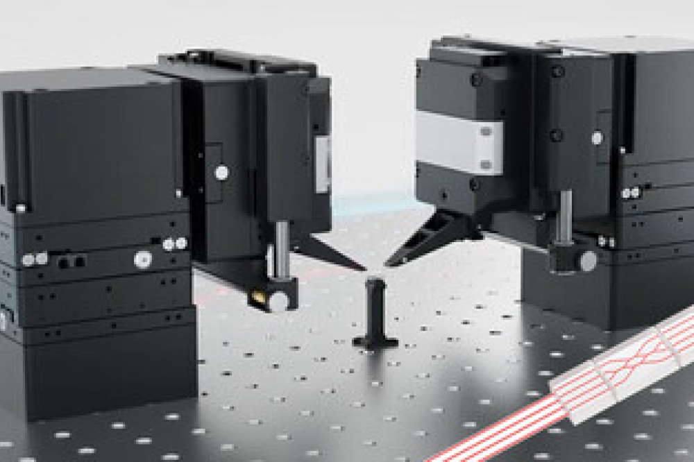
Main image – The double sided fiber alignment systems from PI enables simultaneous positioning of input and output fibers for chip testing and wafer probing. (PI image)
Moreover, the algorithms offer seamless compatibility with today’s photonic devices, which often prove challenging for legacy approaches. For example, there is no implicit assumption of circular symmetry embedded in the algorithms. That posed no issues in 1997, but can be highly sub-optimal for latter-day photonic devices. It can practically be stated that these systems can virtually “optimize anything,” which is definitely not the case for the decades-old approaches still commonly offered.
Image 2 – In the case of the sinusoidal scan routine the defined surface
is scanned continuously without vibration-inducing acceleration or
deceleration phases. Surface, starting point, line distance, and success
criteria can be defined by the user. (PI image)
Image 3 – In the case of the spiral scan routine, a defined area is
scanned helically, whereby either a constant angle or a constant path
velocity is maintained. Its selectable operating frequency helps to
avoid system resonances.
(PI image)
Deeper Dive
Two alignment techniques are most useful today: area scans, and gradient searches for fast optimization and tracking.
Area Scans
A good example of a legacy approach to an area scan is a classical raster or serpentine scan, which sweeps one axis, then increments its orthogonal axis, and repeats until the area is covered. Variations on this theme are common, including stepwise hill-climbs. But these approaches pose fundamental issues today. The stopping-and-starting adds settling time and causes vibration throughout the system, and the linear acquisitions can lead the system to actually de-align in common situations of asymmetric coupling profiles.
Image 4: Ground-breaking results can be achieved with the unique implementation of the gradient search algorithm. If the light signal is present, this gradient search makes it possible to find the signal maximum in typically less than 1 second. (PI image)
By comparison, PI’s firmware-based area scans use smooth, continuous sinusoidal and spiral patterns of selectable frequency. System resonances can easily be avoided, allowing the non-stop scan to proceed without vibration. The result is considerably higher speed. Add built-in modelling in some controllers, and the system can determine the peak (or even the centroid of a top-hat coupling) with good accuracy and speeds down to a few hundred milliseconds.
The digital gradient search was first developed in 1987 and, until now, has been mostly unchanged in its implementation through four subtle generations of the technology. A small, circular motion causes the coupling signal (or other figure-of- merit) to vary, and this variation can be analyzed in phase and amplitude to determine the instantaneous gradient. This allows a fast and direct path to optimum, with tracking possible for appropriate mechanisms.
PI’s radical fifth-generation approach builds on this classical foundation to enable multiple gradient searches to proceed in parallel. For example, this allows an XY lock-on to be performed at the same time a theta-Z optimization runs – an essential combination for any array-device alignment. This fast, parallel execution replaces the time-consuming iterative loop of separate XY and theta-Z alignments that was formerly required. One step, instead of dozens.
Breakthrough
Since 2016, firmware-based fast-area scan, gradient search, and parallel gradient search technologies have been implemented in PI’s powerful piezo nanopositioner and hexapod controllers. Now fast alignment functionality is available for ACS controls. Combined with PI’s large industrial stages (including spindle-driven and linear-motor stages, gantries and air-bearing assemblies), this forms a foundation for especially high-throughput applications involving large-area processing, such as when devices are processed in trays, or across several stations, or on an indexing platform or conveyor.
Image 5 – Example of an automation subsystem for multi-channel automated photonic-device assembly tools, based on the proven double-sided F-712 HA2 alignment system and PI´s multi-axis gantry system. (PI image)
ACS controls lead the industry in modularity and performance. Based on an EtherCAT open, distributed architecture, they support absolute encoders, minimizing system start up times, easing initialization approaches and reducing collision risks. ACS’ yaw control (combined with PI’s highly optimized joint construction) provides industry-leading orthogonality correction and minimizes risk of axis binding – a distressingly common issue for older architectures. True MIMO gantry control plus dynamic cross-axis control yields uniform performance over the gantry area, eliminating grid-based approximation methods and their consequent lowest-common-denominator approach to tuning over large areas. Together, these
mean higher performance and reproducibility in application.
Image 6 – This conceptual demo shows how PI’s fast alignment can apply to large-area applications, such as pick-and-place, and the screening, assembling and testing of photonic devices. From the wafer, through coupon and chip, to the packaged product. (PI image)
These benefits come with PI’s and ACS’ rich offering of global support options, ranging from on-site Quick Start and training, to extended warranties and service plans, to consulting and co-engineering, to application and software consultation and quick-port approaches for key transiting from other architectures.
Summary
Photonics today is serious business, with a rapid rate of innovation and broad adoption by important semiconductor and networking players. Manufacturing and testing these devices demands flexibility and high performance from production systems and tooling.
Multiple studies have spotlighted alignment time as the highest cost contributor to photonic device fabrication, both from the lengthy process times formerly required and from the repeating requirement for alignment throughout the production process. PI’s revolutionary fast alignment technology is unmatched for meeting these challenges, and now it is deployed in large-area mechanisms based on a modular, open-architecture approach ideal for systems integration and tooling platforms.


