

Integrated Photonics Benefit from Emerging Graphene Flagship Programmes
The-EU funded Graphene Flagship is an ambitious programme
begun in 2013 to assist academic and industrial researchers in
transitioning the many promising aspects of 2D graphene technologies
into materials and processes for photonic and electronic applications.
The consortium of 170 research groups in 21 countries recently announced
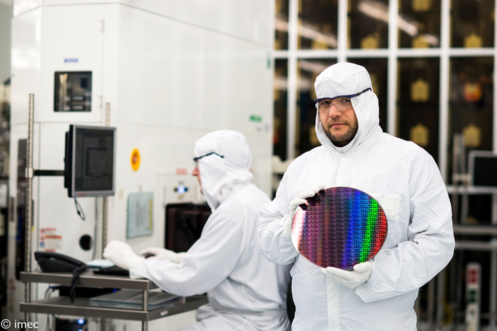
the development of a €20 million experimental pilot lines (EPL)
programme and results that appear foundational to future
graphene-enabled photonics.
By: Mark Andrews, Technical Editor, PIC Magazine
The tantalizing promises of utilizing 2D graphene to manufacture photonic and electronic devices has fueled billion-euro investments across industry and academia. But bringing graphene into practical, widespread use across industries has proved elusive. That old reality appears on the verge of changing as the EU-funded Graphene Flagship project is producing results, peeling back the curtain on what may be a new age of 2D materials across multiple sectors.
Why all the interest in graphene? For starters, graphene is considered by most as the world’s thinnest material at only one atom thick. In its purest form, graphene has many properties of interest to photonic and electronic product developers. Even though 2D graphene is a million times thinner than a human hair, it is incredibly strong, besting steel and diamond gram for gram. Graphene can bring stiffness and durability in myriad applications without the bulk, weight or cost of legacy materials. Yet even though it is strong, graphene is also flexible, which has fueled dreams of using graphene in wearable devices and foldable electronics. Since it is transparent, graphene could support bendable smartphone screens and has wide ranging photonic building block applications including modulators, sensors, and photodetectors. Graphene-enabled photonic devices can absorb light from ultraviolet to far-infrared, with promising applications in ultra-broadband communications. Graphene devices offer ultra-high carrier mobility that can enable data transmission exceeding 100 Gbps.
Enabling the full potential of graphene for European developers and manufacturers is a central goal of the EU’s Graphene Flagship. Recently, the programme provided €20 million to fund experimental pilot lines (EPLs) that will enable a low volume means to test experimental devices on the road to full production. The EPL concept is designed to bridge the gap between lab-scale manufacturing and large volume production.
On 10 February Graphene Flagship researchers announced a new method to integrate graphene and other 2D materials into semiconductor manufacturing lines, an early milestone achievement of the EPL programme. That announcement was followed a day later by news that programme researchers had devised a wafer-scale production technique that could be foundational to new generations of graphene-based photonics.
As programme researchers noted in their announcement, two-dimensional materials have a huge potential for enabling devices with much smaller form factors and extended functionalities with respect to what can be achieved with today’s silicon technologies. But to exploit this potential, manufacturers must be able to integrate 2D materials into semiconductor manufacturing lines – a notoriously difficult step. Researchers in Sweden and Germany now report a new method to make this work.
Details of the new technique were published in ‘Nature Communications,’ which documented efforts from Graphene Flagship partners including RWTH Aachen University, the Universität der Bundeswehr München and AMO GmbH, in Germany, as well as efforts by the KTH Royal Institute of Technology, in Sweden, in collaboration with Protemics GmbH.
“There’s always this critical step of transferring (graphene) from a special growth substrate to the final substrate on which you build sensors or components,” remarked Arne Quellmalz, a researcher at KTH Royal Institute of Technology and lead author of the paper. “You might want to combine a graphene photodetector for optical on-chip communication with silicon read-out electronics, but the growth temperatures of those materials is too high, so you cannot do this directly on the device substrate.”
So far, most documented methods for transferring 2D materials from their growth media to the target substrate are either non compatible with high-volume manufacturing or lead to a significant degradation of the 2D material along with its electronic properties. According to the team, the beauty of the solution proposed by Quellmalz and co-workers is that it lies in the existing toolkits of semiconductor manufacturing: to use a standard dielectric material called bisbenzocyclobutene (BCB), along with conventional wafer bonding equipment.
“We basically glue the two wafers together with a resin made of BCB,” explained Quellmalz. “We heat the resin until it becomes viscous, like honey, and press the 2D material against it.”
At room temperature, the resin becomes solid and forms a stable connection between the 2D material and the wafer, Quellmalz said. “To stack materials, we repeat the steps of heating and pressing. The resin becomes viscous again and behaves like a cushion, or a ‘waterbed,’ which supports the layer stack and adapts to the surface of the new 2D material.”
Researchers demonstrated the transfer of graphene and molybdenum disulfide (MoS2), as a representative for transition metal dichalcogenides, and stacked graphene with hexagonal boron nitride (hBN) and MoS2 to heterostructures. All transferred layers and heterostructures were reportedly of high quality in that they featured uniform coverage across silicon wafers up to 100mm in diameter; after the transfer, the 2D materials showed little strain compared to other methods for moving graphene from its growth substrate to the target wafer.
“Our transfer method is in principle applicable to any 2D material, independent of the size and the type of growth substrate”, says Prof. Max Lemme, from Graphene Flagship partners AMO GmbH and RWTH Aachen University. “And, since it relies only on tools and methods that are already common in the semiconductor industry, it could substantially accelerate the appearance on the market of a new generation of devices where 2D materials are integrated on top of conventional integrated circuits or microsystems.”
“This work is an important step towards this goal, and although many further challenges remain, the range of potential applications is large: from photonics, to sensing, to neuromorphic computing. The integration of 2D materials could be a real game-changer for the European high-tech industry,” concluded Lemme.
Graphene Flagship researchers have also devised a wafer-scale fabrication method that paves the way to creating next generation photonic datacom and telecom devices. As PIC developers and manufacturers appreciate, the classic pluggable transceivers in today’s data centers have limitations in terms of size and cost. An especially vexing issue is power consumption, which is directly related to greenhouse emissions. Graphene could change this and transform the future of broadband communications. Graphene Flagship researchers have devised a wafer-scale fabrication technology that, thanks to predetermined graphene single-crystal templates, allows for integration into silicon wafers, enabling automated manufacturing that in turn paves the way to higher volume production.
Details of the researchers’ work was published recently in the journal ‘ACS Nano,’ and represents the value of collaboration taking part in Graphene Flagship sponsored endeavors. Participants included CNIT and the Istituto Italiano di Tecnologia (IIT), in Italy; the Cambridge Graphene Centre at the University of Cambridge, UK; and Graphene Flagship associate member and spin-off, CamGraphIC. INPHOTEC and researchers at the Tecip Institute in Italy provided the graphene photonic integrated circuits (PICs) used in the study.
The adoption of single-crystal graphene arrays was instrumental in the group’s success, according to study participants.
“Traditionally, when aiming at wafer-scale integration, one grows a wafer-sized layer of graphene and it is then transferred onto silicon,” explained Camilla Coletti, coordinator of IIT’s Graphene Labs, who co-led the study. “Transferring an atom-thick layer of graphene over wafers while maintaining its integrity and quality is challenging,” she added. “The crystal seeding, growth and transfer technique adopted in this work ensures (placement of) wafer-scale high-mobility graphene exactly where it is needed; this is a great advantage for the scalable fabrication of photonic devices like modulators,” Coletti concluded.
By 2023 researchers estimate that the world will see over 28 billion connected devices, most of which will require 5G to maintain connections to various network infrastructure. These challenging requirements will demand new technologies.
“Silicon and germanium alone have limitations; however, graphene provides many advantages,” said Marco Romagnoli from Graphene Flagship partner CNIT. “This methodology allows us to obtain over 12,000 graphene crystals in one wafer, matching the exact configuration and disposition we need for graphene-enabled photonic devices,” he added. Furthermore, the process is compatible with existing fab toolsets and processing techniques, which should accelerate its industrial uptake and implementation.
In a ‘Nature Communications’ article, researchers from Graphene Flagship partners used this approach to demonstrate a practical implementation: “We used our technique to design high-speed graphene photodetectors,” says Coletti. “Together, these advances will accelerate the commercial implementation of graphene-based photonic devices.”
Frank Koppens, Graphene Flagship Leader for Photonics and Optoelectronics, remarked that: “This is the first time that high-quality graphene has been integrated on the wafer-scale. The work shows direct relevance by revealing high-yield and high-speed absorption modulators. These impressive achievements bring commercialisation of graphene devices into 5G communications very close.”
Andrea C. Ferrari, Science and Technology Officer of the Graphene Flagship and Chair of its management panel added: “This work is a major milestone for the Graphene Flagship. A close collaboration between academic and industrial partners has finally developed a wafer-scale process for graphene integration. The graphene foundry is no more a distant goal, but it starts today.”


