

Next-generation Transceiver Testing Starts at Design Planning Stage
The world’s unquenchable bandwidth thirst was already well known by datacom operators and vendors as 2020 began. But the pandemic brought this home like nothing else. Suddenly, people everywhere found themselves working, educating children and living their lives online. A digitized life was no longer a sci-fi movie premise, it was reality. As overloaded networks crashed and numerous consequences of unprecedented demand abounded, the need for advanced PIC solutions was pushed to the forefront of vendor and operator planning.
PIC Magazine asked Francois
Robitaille, Director, NEMs Manufacturing, Design, & Research at
EXFO, to share his insights about what is happening at the design phase
for transceiver testing and what trends he experts as 2021 unfolds.
Network equipment manufacturers (NEMs) and service providers around the world are forging ahead with deployment of advanced technologies including 5G mobility, 400 Gbps and even 800 Gbps fiber optic networks. This rapid proliferation of next-generation networking technologies is causing a boom in demand for optical transceivers, as documented by recent market reports such as Light Counting’s market research of 2020.
Light Counting forecasts strong global growth for optical transceivers, with acceleration in revenue growth of more than 20 percent projected for this year. NEMs everywhere are challenged with producing – and testing – thousands of transceivers and active optical cables (AOC) daily. Component vendors need more efficient test methods than ever before to keep pace with this burgeoning demand and to accommodate new optical component characteristics.
Q. Francois, what do you see happening with regard to advances in transceiver technology?
A. As you’ve mentioned, it’s evident that the demand for transceivers is booming globally. In response, Photonic Integrated Circuits (PICs) have become the cornerstone for high-speed communications driven by 100 Gbps and 400 Gbps optical transceiver requirements for telecom and data centers. PIC technology is about to revolutionize the components industry by enabling a mix of optical and electronic functionalities on a single chip, reducing size, power consumption, and cost while boosting reproducibility and yield. Several vendors have recently launched the first of their PIC solutions and I anticipate demand for transceivers based on PIC technology to increase exponentially in 2021 and beyond.
Q. Is the evolution to silicon photonics something that will become the norm or a niche within components manufacturing?
A. Silicon photonics is absolutely going to change the way optical systems are designed and built going forward. PICs will become ‘table stakes’ if NEMs want to remain competitive. With hyperscale datacenters expanding and 5G driving the proliferation of transmitters, the only way to meet that exponential demand will be to use PIC based solutions to reduce component size and lower power consumption. In fact, all sectors that use light for transmission including LiDAR, medical applications, sensing, the Internet of Things (IoT), and even quantum computing will need to adopt PIC technology to remain viable.
Q. As manufacturers adopt silicon photonics what challenges could they encounter?
A. The high volume of components that will require testing coupled with the need for efficient and accurate testing at every stage of design, fabrication and packaging has inherent challenges for manufacturers. The primary goal in 2021 is to speed time-to-market for component manufacturers without compromising quality. To deliver peak performance, test solutions are needed to ensure the efficiency of PIC testing at the starting point -- which is the design planning phase.
A key trend this year will be the shift in mindset from focusing on testing the finished product, to testing at the wafer and the die level to ensure viability from the get-go. Next-generation transceiver testing starts at the design stage. By designing to test rather than testing after the fact, there are multiple benefits. Identifying issues at the wafer level can save thousands of dollars because faulty components are identified as early in the process as possible – before the packaging stage. The savings are impressive given that 70 to 80 percent of PIC-based device costs are incurred from packaging as compared to 20 to 25 percent for silicon electronics.

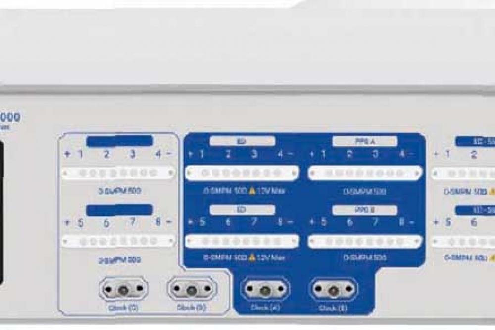
EXFO-MA-4000 Module Analyze
Q. Can you tell us about what needs testing during the manufacturing process and why?
A. NEMS need to develop their testing strategy during the design phase so that the type of testing required, access and injection points, how tests will be simulated and still more factors are taken into consideration in advance of production and testing. It’s important to implement testing points and capabilities in the component design.
There are two types of testing to keep in mind when planning: die-level tests that perform parametric qualification of internal components; and functional testing for quality control, performed after the transceiver is produced. Of key importance during the manufacturing phase is ensuring compliance with industry specifications and standards.
As noted above, the earlier that testing can be conducted in the process, the more cost-effective and efficient the outcome. What we’re seeing tested today ‘post-packaging’ is quite different from what we’ll see in the near future with increased testing earlier at the die and wafer stage. Even some functional tests will happen earlier in the process than what occurs today. This will enable identifying faulty components as early as possible in the manufacturing process.
Ultimately, component manufacturers are looking for a streamlined approach for fast, accurate validation of electrical and optical testing. Testing needs to be comprehensive, providing coherent end-to-end solutions for repeatable and accurate results wherever testing is done.
Q. What does that end-to-end testing solution for labs and manufacturing look like?
A. End-to-end transceiver qualification – and especially testing at the die-level stage – requires a complete range of high-end optical and electrical testers. To help transceiver vendors ensure compliance throughout the transceiver lifecycle, EXFO recently expanded its range of electrical and optical test solutions by acquiring InOpticals Inc., a technology leader providing ultra-high-speed test instruments for the lab and manufacturing markets.
InOptical’s solutions are being integrated into EXFO’s test & measurement product line to deliver comprehensive, modular test solutions. That will bring best-in-class performance across the end-to-end process for transceivers and optical components based on PICs. This is an exciting advance in delivering the capability of test solutions at the lab design stage that can potentially speed up quality component manufacturing processes.
Here are some of the new products now available from EXFO:
• BA-4000: 400G/800G electrical bit-error-rate (BER) tester
• MA-4000: the most compact solution in the industry that combines a BER tester and a module compliance board (MCB)
• EA-4000: high-performance and ultra-fast electrical/optical sampling scope.
These testers complement EXFO’s expertise in optical testing to provide highly reliable and fast transceiver qualification, leveraging best-in-class testing performance from end-to-end.
Q. Where do you see the market headed in 2021?
A. This year we will certainly see wider adoption of silicon photonics and exponential availability of commercial components based on new silicon photonics technology. An opportunity in 2021 and beyond is to make better use of test data acquired during manufacturing to optimize the entire process, possibly using AI capabilities. So much information collected during testing is currently discarded or filed. I anticipate that NEMs will find ways to mine that data, which could then inform decisions for design, testing, and manufacturing; I believe this will benefit the optical industry as a whole.


About the author:
François Robitaille joined EXFO in 2000. His main
responsibilities include NEM market assessment, identifying potential
growth areas and key product ideas as well as ensuring that products
reach the market and are commercially successful. François started his
career as a Project Manager for Gentec Electro-Optics and from there
moved to Bell Mobility Radio in Engineering and Sales, then to Davicom
Technologies as Director of R&D. François holds a Master's Degree in
Electrical Engineering from Université Laval, in Quebec City. He brings
extensive expertise in both R&D and sales to EXFO.
For more
information about designing, testing, and validating the next generation
of transceivers, download EXFO’s flyer and view the recent webinar.


