

Super-fast optical interconnects
Universal chip-to-chip optical interconnects are delivering off-package
communication at the bandwidth density and energy cost of in-package
electrical incumbents.
BY VLADIMIR STOJANOVIC FROM AYAR LABS
Data dashes through today’s optical fibre system networks before it slows to a crawl at copper interconnects. These bottlenecks occurs at copper pins and wires on circuit boards, where electrons transmit data at far lower speeds. So great are these delays that there will come a time when copper interconnects will have to be replaced by optical signalling.
Offering a universal solution to this issue is our team from Ayar Labs of Emeryville, CA. Founded in 2015 as a spin-out of three universities Massachusetts Institute of Technology; University of California, Berkeley; and University of Colorado, Boulder we are renowned for our pioneering work in micro-ring chip architectures.

Figure 1. Large penalties will be incurred for leaving the chip,
package, and board (source: Gordon Keeler, DARPA MTO, ERI Summit 2019).
We have developed a chip-to-chip optical input/output (I/O) interconnect technology that addresses several weakness associated with electrical interconnects and their scaling limitations. We tackle weaknesses associated with signalling speeds and pin count, which both apply the brakes to electrical I/O connections, and power consumption that is increasing at an unsustainable rate.
The latter concern should not be taken lightly, as it will not be long before the power drawn by the off-chip I/O will account for almost all the power consumption of the package. When this occurs, it will be infeasible to use of electrical I/O interconnects, which are primarily made of copper. By then, there will need to be have been a shift to chip-to-chip communications based on photonics, a technology that will eliminate electrical I/O bottlenecks.
Introducing new photonic I/O architectures will also satisfy growing throughput demands. There is an emergence of heterogeneous computing, involving central processing units (CPUs), graphic processing units (GPUs), field-programmable gate arrays (FPGAs), neural network accelerators, and resource pooling on the memory side. This trend demands more I/O at the application level, while electrical I/O is running into pin count, signalling and power limitations.
Providing an impetus to act sooner rather than later, the penalties for leaving the chip, package, and board are on the up (Figure 1). This begs the question: will the 112-Gbit/s serializer/deserializer be the last long-range electrical I/O solution? In field deployments, system integrators are already seeing the limitations of 112-Gbit/s long-range electrical connections they are incapable of spanning the signalling lengths required for off-board, rack-scale communication.
To evaluate the performance of the I/O technologies, we use a figure of merit involving quite a few terms. It considers the bandwidth density from the edge of the I/O solution, multiplied by its associated energy efficiency. This provides a yardstick that captures the Gbit/s per millimetre per pJ/bit, as a function of distance. When crossing the boundaries from package to board with I/O technologies, this metric plummets – there is a gap of about four orders of magnitude between in-package interconnect solutions and state-of-the-art optical solutions that provide off-board connectivity.
Into this challenging space comes our new optical I/O technology. It delivers a universal I/O solution that provides off-package communication at the bandwidth density and energy cost of in-package electrical incumbents.

Figure 2. Ayar Labs’ in-package optical I/O system architecture (source: Ayar Labs).
An in-package solution
To pull off an optical I/O, certain requirements must be fulfilled (see Figure 2). We meet them with our own optical I/O system architecture. This is a chiplet-based solution that is co-packaged directly with the host system-on-chip (SOC) within a multichip module (MCM) package. By incorporating a monolithic electronic-photonic CMOS chiplet, which we call TeraPHY, we realisea flexible electrical I/O interface adapted to the host SOC, whether the geometry is wide parallel or high-speed serial. Adopting this approach offers flexibility, giving a choice between a silicon interposer and an organic substrate for the package.
One of the merits of our single-chip solution is that it enters a manufacturing ecosystem already established for MCMs. With our architecture, we keep the laser supply outside the module. This simplifies packaging, improves laser reliability, and alleviates issues related to the operational temperature mismatch of SOC packages and laser optical supplies. Due to these advantages, we realise further integration of lasers into a multi-port, multi-wavelength laser module solution, which we refer to as SuperNova.

Figure 3. Six areas must be addressed to make in-package optical I/O a reality (source: Ayar Labs).
Several system and technology requirements have to be met for in-package optical I/O to become a reality (see Figure 3). At the system level, the optical I/O requires high-density optical devices and circuits capable of fulfilling the high-bandwidth density demands of future SOCs and applications.
To ensure success, it is critical to draw on existing CMOS processes and manufacturing infrastructure, while complying with I/O standards. And, perhaps most importantly, production must leverage scalable, high-volume manufacturing of the semiconductor technology.
We meet these requirements with wavelength-division-multiplexed (WDM) links that support multiple wavelengths per fibre and allow scaling of the data rate to meet the bandwidth density requirements of future applications. We use closely spaced wavelengths – they are separated by a few hundred GHz – running concurrently on the same fibre. Transmitters and receivers modulate/receive each wavelength separately.
By leveraging monolithic integration and the CMOS process, we create a chiplet-driven technology with tight integration of electronics and photonics while improving bandwidth-density and energy metrics.
Finally, our monolithic approach taps into the ecosystem of CMOS foundries and scalable high-volume packaging manufacturing of multichip modules. Thanks to this, we have created a compatible solution for advanced packaging and fibre attach.

Figure 4. The TeraPHY optical I/O architecture, centred on a micro-ring modulator and WDM (source: Ayar Labs).Optimising the optical architecture
At the heart of our optical I/O architecture lies micro-ring modulator and WDM technology (see Figure 4). At its crux is an off-chip continuous-wave laser, based on non-proprietary standards. This emitter is driven by the continuous-wave WDM Multi Source Agreement (CW-WDM MSA), which provides optical power in one or more wavelengths to the TeraPHY chip. Light enters this chip through a coupler and then travels along it in an optical waveguide. The light encounters a micro-ring modulator, which converts data from an electrical domain to the optical domain.
Our micro-ring has a very narrow resonance, typically just 20-40 GHz that is repeated at a much larger period, such as 3.2 THz. With these conditions the micro-ring is wavelength selective. This allows the micro-ring modulator to act as both a modulator and a wavelength division multiplexer, enabling the addition of more wavelengths to the same fibre/waveguide. By making our micro-ring modulators out of silicon, we are employing the same material used to produce all the transistors and optics on the chip.
Output from our chiplets is coupled to the fibre and sent to the receiver chips. Here, micro-ring detectors convert data from the optical domain to the electrical domain. Micro-ring detectors actually perform a dual role, combining the tasks of detector with that of wavelength-division demultiplexer, picking the selected modulated wavelength for the receiver.

Figure 5. Wavelengths can be added to the fibre – without increasing
the strain on the backend electronics – to improve energy-efficiency,
bandwidth density and overall throughput of the fibre (source: Ayar
Labs).
We can increase the bandwidth density of our links, alongside the overall throughput of the fibre, by adding wavelengths to the fibre. It’s an improvement that we accomplish without increasing strain on backend electronics. Using cascaded micro-rings as independent communication channels, we realise up to 64 micro-rings per fibre. This yields a technology that provides up to 6 to 8 Tbit/s per fibre (see Figure 5).
Drawing on this development and others, we have constructed a complete WDM link system, formed by integrating electronic and photonic components. Electronics modulates and receives the data and controls micro-ring resonances through thermal tuning and wavelength locking (see Figure 6). With our technology, transmitter ring modulator resonances are locked to incoming laser wavelengths, prior to locking of the receiver. Working together, locking loops track local and global temperature fluctuations while compensating for process-induced wavelength grid non-idealities that occur in the laser, transmit and receive chips.

Figure 6. A complete WDM link system that integrates electronics with photonics components (Source: Ayar Labs).
Our interconnects excel in bandwidth density and energy efficiency, thanks to miniaturisation of the micro-ring devices, which are integrated with CMOS transistors. The link architecture has enabled us to create TeraPHY, which is essentially a chiplet that provides Tbit/s optical connectivity and offers an alternative to electrical serializer/deserializer chiplets.
The main features of our demonstration chiplet are: a 24 channel advanced interface bus (AIB), providing a total data bandwidth of 906 Gbit/s; ten photonics Tx/Rx macro pairs, configurable to 125 Gbit/s to 256 Gbit/s per macro that equates to 1.28 Tbit/s to 2.56 Tbit/s per chip; a non-return to zero modulation format for the optical channel, eliminating the need for forward-error correction; a reach of up to 2 km; and an all-inclusive estimated energy efficiency of less than 5 pJ/bit.
Figure 7. The TeraPHY chiplet with mixed-pitch bumps (source: Ayar Labs).
Our TeraPHY chiplet operates like an electrical chip. To ensure this, we use a variety of pitch bumps – there is a combination of a tight 55 µm-pitch for the AIB interface standard, and a mixed pitch, because our chiplet uses a variant of an embedded multi-die silicon interconnect bridge (see Figure 7). With this arrangement, the main die is connected to others via a piece of silicon. It has been embedded within an organic substrate to provide fine-line connectivity using a 55 µm-pitch for the bump between the die. This enables fine-pitch 2.5D-type packaging without having to use a silicon interposer. Instead of that we can use an organic substrate, which provides greater flexibility in terms of area and yield.
A major selling point of our in-package chiplet is that it provides a universal off-package interconnect solution for any SOC, including FPGAs, CPUs, GPUs, tensor processing units and switches. Applications include: radar; disaggregated resources for data and high-performance computing racks; 5G connections between front-panel RFIC array and back-end digital beam-forming processors; and artificial intelligence compute scale out, such as GPU to GPU, TPU to TPU, FPGA to FPGA, and CPU to GPU.

Figure 8. Multi-chip package assembly with in-package optics (source: Ayar Labs).
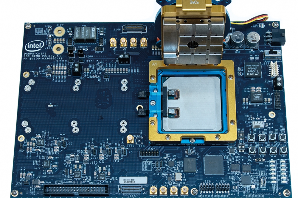
Delivering demonstrations
Back in March 2020 we provided a live demonstration of our chiplet technology. Working in partnership with Intel under the U.S. Defense Advanced Research Projects Agency’s (DARPA) Photonics in the Package for Extreme Scalability (PIPES) programme, we replaced the traditional electrical I/O of a state-of-the-art FPGA with optical signalling interfaces.
This effort, which drew on Intel’s advanced packaging and interconnect technology, involved the integration of TeraPHY optical I/O chiplets and an Intel FPGA core within a single package to create a MCM with in-package optics (see Figure 8). This MCM substantially improves interconnect reach, efficiency, and latency – and ultimately enables high-speed data links featuring single-mode optical lasers coming directly from the FPGA.
The optical waveguides on our chiplet, which are patterned monolithically into the silicon, are the optical equivalents of copper wires. When we bring two waveguides in close proximity, we can transfer photons and power from one waveguide to another to create a coupler. Within the coupler, a 10-µm diameter micro-ring resonator electrically modulates the light’s phase and controls its direction. Light is either let through, directed to a drop port, or allowed to dissipate inside the micro-ring.
We use GlobalFoundries’ 45 nm-platform for CMOS chip manufacturing. This supports the construction of our co-packaged chiplet that provides an I/O bandwidth of 2 Tbit/s, realised at a small fraction of the power compared with an electrical I/O.

Figure 9. Application areas for advanced integrated circuits with photonic interfaces (source: Gordon Keeler, DARPA, ERI Summit 2020).
DARPA’s PIPES programme is targeting development of advanced integrated circuits that feature photonic interfaces capable of driving bandwidths greater than 100 Tbit/s I/O per package at energies below 1 pJ per bit. Deploying interfaces with this level of performance in FPGAs will improve high-performance computing, AI, large-scale emulation, and U.S. Department of Defense capabilities, such as radio-frequency arrays, advanced radar, and 5G (see Figure 9).
Our demo featured eight wavelength-division-multiplexed channels per macro, using I/O data rates of 16 Gbit/s/wavelength across four optical macros on a single chip. This provided connectivity at 512 Gbit/s.
The demonstration involved low-power signalling standards and chiplet packaging processes developed by Intel for another DARPA programme. This work also used Intel’s common interface standard, known as AIB. It is a publicly available, open interface standard that enables us to integrate the MCM and in-package optics.
In production, our single chiplet is expected to reach up to 2 Tbit/s I/O over 64 wavelength channels, at 32 Gbit/s per wavelength. There is no need for forward-error correction, and latency is less than 10 ns. Our chiplet is also designed to work with an off-chip multi-wavelength continuous-wave laser source and integrate with any type of partner system on package – this could be a CPU, GPU, ASIC, or FPGA – to connect switches, servers, and cards over distances up to 2 km.

Figure 10. In a single-die package demo, Ayar Labs demonstrated 25 Gbit/s transmitters and 25 Gbit/s receivers with an aggregate bandwidth of 800 Gbit/s on the transmitter side (source: Ayar Labs).
Beyond our work with DARPA and Intel, we are continuing to advance our in-package optical I/O technology. In a single-die package demonstration this July we took another step forward, highlighting that our micro-ring-based WDM can meet the requirements for next-generation high-performance chip-to-chip I/O. This effort showcased 25 Gbit/s transmitters and 25 Gbit/s receivers, with noteworthy accomplishments including an aggregate bandwidth of 800 Gbit/s on the transmitter side and a bit error rate below 1 x 10-12 on the receiver side (see Figure 10). Combined, energy efficiency came in at just 4.91 pJ/bit.
This demonstration is a milestone on our path towards showcasing the full capabilities of our chiplet. By running each wavelength channel at 32 Gbit/s, our single chiplet can deliver an aggregate bandwidth of 2 Tbit/s for transmit and receive.
We plan to roll out a 2 Tbit/s TeraPHY chiplet. But that is just the beginning of the roadmap for our technology – we will trailblaze a path to 32 Tbit/s per chip, realised at just 1 pJ per bit.
The road ahead
By producing our devices using monolithic in-package optics, we are in a unique position to leverage both the existing chiplet ecosystem and the high-volume manufacturing of MCM assembly approaches. Thanks to the use of the same package for the optics, we are not shackled by the traditional distance trade-off in energy efficiency and bandwidth density. This opens the door to new high-performance computer architectures with off-package communication at the cost, energy, and bandwidth density of in-package interconnects.
It is worth emphasizing that the key to realising this chip, featuring integrated photonics and electronics on the same die, is the monolithic integration of photonic components. This approach bore much fruit in the university research that laid the foundations for our company, and through further development, it is now allowing us to make further breakthroughs. We are now refining a technology where photonics components are directly integrated with advanced transistors in a 45 nm process to create complex electronic-photonic systems, such as WDM links.
Using this approach, we can create single CMOS wafers that contain chiplets that integrate photonic components with transistors to support a wide variety of electrical interfaces.
Compare our approach with that of our peers and you’ll see that many of the SOC manufacturers have come up with MCM technologies that are driven by the need to realise mixed-die functions on complex applications, such as GPU, CPU, memory, or I/O. One major drawback of that type of approach is that these functions require diverse processes and process nodes – whether it is a DRAM node or a CMOS node in 10 nm or 7 nm technology, and the complexity of MCM assembly is more cost-effective than the development of a process that encompasses all the features required by all the functions. Additionally, even for the same functions, the MCM approach enables significant cost reduction through yield improvement by breaking-up a large die (e.g. 64 core microprocessor) into smaller dies that yield better (e.g. eight 8-core dies).
We are now starting to sample our first TeraPHY chiplet generation with select partners. This is the beginning of a journey, which will continue to new generations of the chiplet. We plan to advance our technology with electrical interface variants that address different host SoC needs and packaging scenarios, and deliver greater throughput by increasing the number of wavelengths and the data rate per wavelength. Target applications exist within artificial intelligence, supercomputing, data centres, aerospace, defence, telecom, and eventually autonomous vehicles.
This research was developed with funding from the Defense Advanced Research Projects Agency (DARPA). The views, opinions and/or findings expressed are those of the author and should not be interpreted as representing the official views or policies of the Department of Defense or the U.S. Government.
Further Reading
Ayar Labs Technical Brief: Optical I/O Chiplets Eliminate Bottlenecks to Unleash Innovation (see https://ayarlabs.com/technical-brief-optical-i-o-chiplets-eliminate-bottlenecks-to-unleash-innovation/)
Paradigm Change: Reinventing HPC Architectures with In-Package Optical I/O (see https://ayarlabs.com/paradigm-change-reinventing-hpc-architectures-with-in-package-optical-i-o/)
TeraPHY: A Chiplet Technology for Low-Power, High-Bandwidth In-Package Optical I/O (see https://ayarlabs.com/teraphy-a-chiplet-technology-for-low-power-high-bandwidth-in-package-optical-i-o/
TeraPHY: An O-band WDM Electro-optic Platform for Low Power, Terabit/s Optical I/O (see https://ayarlabs.com/download/teraphy-an-o-band-wdm-electro-optic-platform-for-low-power-terabit-s-optical-i-o/)


