Graphene to enable new generations of PICs

The possibilities of incorporating the unique electrical, physical
and photonic properties of graphene into photonic integrated circuits
has appealed to PIC developers since harvesting the 2D material was
shown possible by two Russian physicists in 2004. Those physicists,
Andre Geim and Kostya Novoselov, won the Nobel Prize in 2010 for their
work with graphene. EPIC reports on advances being made to bring the
potential of graphene into production across Europe and the UK.
Ivan Nikitskiy, Photonics Technology Expert, European Photonics Industry
Consortium (EPIC)
With its unique optical and electrical properties, strength, lightness, and thinness, graphene is seen as an ideal material to produce the next-generation of faster and more efficient electronic and photonic devices required to support the exponential growth in global data traffic for datacom and 5G industries.
In this article, we look at the development and commercialization of graphene optoelectronics in Europe and the challenges that need to be addressed to realize the large-scale integration of graphene into photonic integrated circuits.
Graphene is the name given to a flat monolayer of carbon atoms or a two-dimensional (2D) form of graphite with a honeycomb lattice structure. Although the theoretical study of atomically thin carbon structures started almost 100 years ago, atomic monolayer materials have been known only as an integral part of larger 3D structures, usually grown epitaxially on top of monocrystals with matching crystal lattices. 2D materials were presumed not to exist in the free state, being described as purely academic models. However, in 2004, these academic models were suddenly turned into reality, when free-standing graphene was unexpectedly discovered by two Russian physicists, Andre Geim and Kostya Novoselov, who were the first to study its unique material properties experimentally, along with demonstrating the possibility to obtain a variety of other materials in their free-standing 2D form. In 2010 they were awarded the Nobel prize in physics, and the rise of graphene had begun1.
Pure graphene is the thinnest, lightest, and strongest material yet discovered that is also flexible, almost transparent, and possesses ultra-high electrical and thermal conductivity. For this reason, graphene was heralded as a wonder material for applications in composites and coatings, transparent and flexible electronics, solar panels and batteries, drug delivery and DNA sequencing. But above all, the exceptional photonic properties of graphene make it ideal for ultrafast optical and data communication components, enabling ultrahigh spatial bandwidth density and low power consumption board connectivity and connectivity between data centres. Furthermore, the ultimate thinness of graphene facilitates its compatibility with modern silicon-based optoelectronics and suggests itself as the platform for the next generation of Photonic Integrated Circuits (PICs)2.
EU initiatives
Discovered in Europe, graphene quickly became one of Europe’s priorities in lab-to-fab technology transfer and recognizing the material’s potential, in 2013, the European Commission set up the GRAPHENE FLAGSHIP project. With funding of
€1 billion over 10 years, Flagship’s mission was to take graphene and related layered materials, from the laboratory to industry with the aim of revolutionizing multiple industries and creating economic growth and new jobs in Europe.
2D-EPL: The Flagship’s most recent initiative has been the launch of the Two-Dimensional materials Experimental Pilot Line (2D-EPL) to integrate graphene and Graphene Related Materials (GRM) in semiconductor platforms. Here, it needs to be pointed out that, in recent years, a large variety of other 2D materials were obtained using scalable synthesis methods with electronic properties ranging from semimetals, direct- and indirect-bandgap semiconductors, to superconductors.
Accordingly, 2D-EPL‘s mission is to bridge the gap between lab-scale manufacturing and large volume production of optoelectronic devices based on graphene and GRM. Starting in 2020, with funding of €20 million, the 4-year project aims to establish a European ecosystem for prototype production of 2D-based electronics, photonics, and sensors.
The project is built on two pillars: one, offering prototyping services in the form of Multi-Project Wafer runs as well as tailor-designed integrations for 150 mm and 200 mm wafers; and the other, the development of a fully automated process flow on 200 mm and 300 mm wafers, including the growth and transfer of high crystal quality graphene and GRM. With 11 partners, covering the whole value chain, including tool manufacturers, chemical and material providers, and research foundries, 2D-EPL is providing prototyping services not only to the core Graphene Flagship project but also to external partners.
METROGRAPH: As part of their Spearhead Projects. i.e., industry-led initiatives aimed to increase the Technology Readiness Level (TRL) of graphene-based technologies, in 2020, the Graphene Flagship launched METROGRAPH to develop a graphene-enabled optical transceiver. In view of the rapidly growing market for PICs and the associated need for integration in high bandwidth communications, the aim of the project is to develop a wavelength agnostic, coherent optical transmitter and receiver based on graphene photonic chips for low-cost, high bandwidth communications. The device will operate at 200 Gb/s in the conventional band and long-wavelength band, covering the 1530–1625 nm wavelength range. The graphene-based photonic circuits will be packaged and tested both in the lab and in a network line card with a TRL of 8, together with a state-of-the-art digital signal processor. Their functionality will be demonstrated in equipment for metro and metro-regional distances of 200 to 1000 kilometers.
R&D: The largest European research center working with the Graphene Flagship is the Belgium-based Interuniversity Microelectronics Centre (IMEC), an international research & development organization, active in the fields of nanoelectronics and digital technologies. Together with National Interuniversity Consortium for Telecommunications (CNIT) in Italy, IMEC develops the work package on wafer-scale integration. This work package targets the transition from laboratory to wafer-based fabrication technology. As Cedric Huyghebaert, program manager of exploratory materials and modules at IMEC and the 2D-EPL division leader, explains: “Many graphene-based concepts have been successfully demonstrated. But most of the demonstrations are limited to the lab and use graphene in the form of small, exfoliated flakes. The real challenge is to mature these concepts from flake-based devices towards real marketable products. And this requires the integration of the material at the wafer scale, in a real production environment”.
Another research organization participating in the Graphene Flagship is AMO GmbH, a non-profit research-oriented nanotechnology SME located in Aachen, Germany, that provides a range of services from consulting to prototype development. With a 400 sqm state-of-the-art cleanroom, AMO’s mission is to efficiently close the gap between university research and industrial application. In recent years, the company has become a global player in 2D materials research for electronics and photonics. In the framework of the 2D-EPL project, AMO will provide two multi-project wafer (MPW) runs where universities, research institutes, and companies can include their designs as dies on joint wafers.
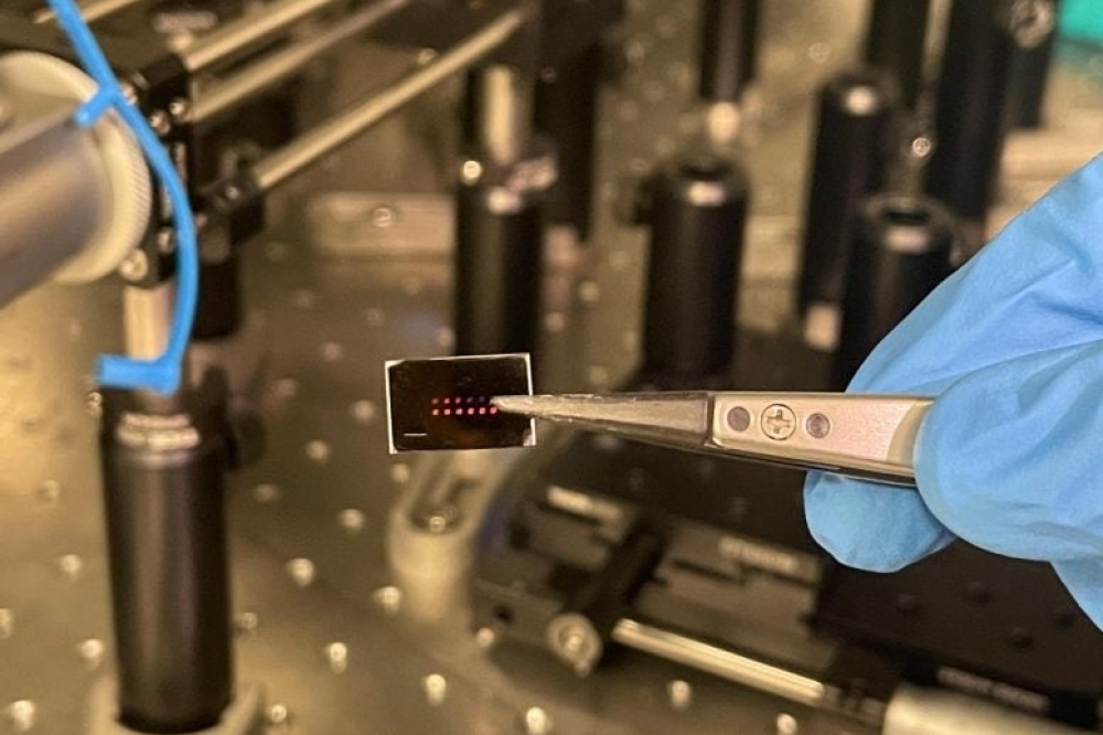
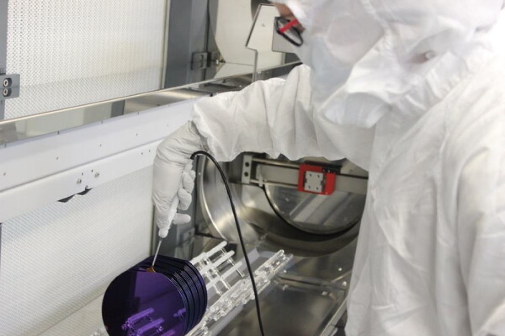
Figure 2 Wafer-scale graphene production
(Courtesy of Graphenea)
Industry of graphene wafer-scale production
Headquartered in Germany, AIXTRON is one of the world’s leading suppliers of deposition equipment to the semiconductor industry and is a key partner of the 2D-EPL initiative. As one of the tool manufacturers, AIXTRON is responsible for developing the growth and transfer tools, as well as processes necessary for graphene and GRM production. AIXTRON has developed a Metal-Organic Chemical Vapor Deposition (MOCVD) reactor for the growth of graphene and GRM directly onto large substrates – up to 300 mm – using its proprietary Close Coupled Showerhead® technology. Direct growth allows industrial-grade 2D materials and their associated heterostructures to be grown insitu for front-end applications. For effective back-end integration, AIXTRON is investigating novel processes as well as developing an automated transfer system of 2D material structures onto device wafers. These platforms will provide key capabilities for the pilot line in realizing large-scale integration of graphene and GRM into logic, memory, photonic, and sensor devices.
Spanish Graphenea is a graphene producer serving just over 800 customers in 55 countries. Its portfolio of products consists of graphene films produced by wafer-scale Chemical Vapor Deposition (CVD), graphene oxides, chips with graphene field-effect-transistors, and graphene foundry services. Around 65% of Graphenea’s activities are related to medical biosensors, the other 35% to photonics devices such as photosensors and optical switches. Graphenea’s most important products are foundry services that follow a pure-play model based on a vertical integration scheme. This enables the graphene to be grown, transferred, and processed under the same roof, which allows the manufacturing process to be continuously monitored and the delivery of high-quality, reliable graphene-based devices, tailored to the customer’s needs.
Founded in 2012 in the Netherlands, Applied NanoLayers (ANL) is a high-volume foundry and producer of GRM sheets with a low defect density such as hexagonal boron nitride for BEOL silicon integration. As ANL points out, CVD growth of graphene is the only technique that can compete with exfoliation when it comes to the electronic properties of graphene, and their advanced CVD systems enable optimum film morphology for wafers from 50 to 200 mm in diameter. Additionally, CVD scales to industrial high-volume wafer-scale series production, where the quality of each graphene sheet can be continuously controlled. Their wafer-scale cold film transfer of 2D materials including graphene and hexagonal boron nitride enables integration with existing substrates such as Si, GaAs, and InP.
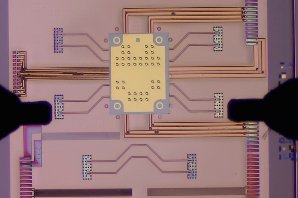
Figure 3 Wafer with integrated circuits comprising 2D materials (Courtesy IMEC)
Industry of graphene integrated photonics
British Paragraf based near Cambridge, is currently producing commercial-quality, graphene-based electronic devices using contamination-free technology that is both scalable and compatible with existing electronic device manufacturing production processes. They have developed a novel production process whereby graphene can be produced directly onto semiconductor-compatible substrates such as silicon, silicon nitride, silicon carbide, and many dielectric materials, making the process suitable for commercially viable electronic devices. Using this technology, Paragraf has been able to integrate high purity graphene in sensors, also aiming to develop solid-state devices, such as transistors and optical modulators as their high electron mobility graphene offers a mass-manufacturable route to producing these devices at scale.
Also based in Cambridge, CamGraPhIC, is set to improve optical communications in data centers and 5G infrastructures. Their core product is a graphene photonic chip for data conversion that, with small variations dependent on applications, constitutes a single platform for datacom and telecom industries.
The aim is to integrate graphene modulators and photodetectors into silicon chips, exploiting graphene’s unique performance across multiple telecommunication bands (1280 – 1310nm, 1525 – 1565nm, and 1565 – 1610nm). Their Graphene Integrated Photonics (GIP) technology platform aims to enable next-generation high-performance up to 200 Gbps, low-cost, and low-power consumption optoelectronic devices. CamGraPhIC is managing INPHOTEC, a high-tech R&D and prototyping center located in Pisa, Italy, which includes a 550 sqm cleanroom. The graphene is synthesized through a CVD process in a single crystal or continuous film format, and the facility makes available several technology platforms such as silicon photonics, graphene photonics, glass, SiN photonics, LNOI, and advanced photonic packaging.
Black Semiconductor based in Aachen, Germany, is developing a technology that allows mass production of high-performance photonics on any electronics enabling ultra-fast data transfer on-and-off chip or performing photonic signal processing, as used in AI systems. Their approach holds great promise for a radically new generation of energy-efficient and high-performance microchips that will enable ultra-fast CPUs, GPUs, and AI systems.
Additionally, Black Semiconductor is developing the first integrated super-chip, combining electronic and photonic circuits in a uniform mass production process without bonding. The approach is compatible with existing machines and technology in the established silicon foundries, which, together with integration into the back-end of chips, is a unique feature of their cost-efficient graphene photonics.
The future
While market reports vary, all predict a rapid growth in the global graphene electronics market over the next 5 years. As an example, Market Study Report forecasts a growth from USD 296.5 million in 2019 to USD 613.1 million by 2025, a CAGR of 19.9%3. Market drivers focus on graphene’s unique properties that will be required for faster and more efficient electronic devices needed to support the rising adoption of IoT applications and the exponential growth in global data traffic. More importantly, existing technology platforms, including the emergent silicon photonics, will not be able to support current roadmaps due to intrinsic technological limitations.
But if these forecasts are to become a reality, several challenges need to be addressed. Firstly, since many of the promising graphene-based photonic and optoelectronic devices rely on single-layer graphene, manufactured using CVD, it is crucial to find solutions to the technological challenges that still exist. For example, how to optimize high-quality growth, transfer tools (which can guarantee high yield and integrity), and processes to fabricate devices at the wafer scale. There are also challenges resulting from the reluctance of the industry to accept new disruptive technology. In this sense, some of the target markets for graphene-based photonic devices can be classified as quasi-monopolistic, where new, disruptive technologies are seen as risks for suppliers. Finally, as with many other photonics technologies, there is a need for standardization, for example, terminology, characterization, processes, and quality control. Without this, it will be difficult to fabricate high-quality graphene-based devices and ensure reliable communication along the supply chains.
More specifically, for Alessio Pirastu, CTO of CamGraPhIC, what is needed is a clear prototyping path for performance validation; an early definition of the technology validation protocol; and early planning or desired qualification activities. Additionally, about scaling up in manufacturing, he sees a need to define what can be done in existing CMOS-compatible fabs, for example, via process design kits (PDKs) for monolithic integration of CMOS electronics with graphene-based photonics. Also important is the need to solve the technical problems that graphene photonics manufacturing might face in the mid-term, such as high-quality graphene, cross-contamination, scalability, and costs. Finally, several fabrication solutions should be implemented (e.g., continuous graphene film, single-crystal graphene) to enable the development and deployment of multiple technical solutions.
While these challenges should not be underestimated, the achievements to date are promising. Firstly, fostered by the Graphene Flagship, there is now an established ecosystem that coordinates nearly 170 academic and industrial partners in 22 countries and has more than 90 associated members in its various projects. With its industry-led initiatives aimed to increase the TRL of graphene-based technologies, this ecosystem is now well placed to resolve many of the technical challenges mentioned above. Secondly, several companies are already working their way towards commercialization in Europe, many of them already as members of EPIC - European Photonics Industry Consortium. These include several spin-offs created by Graphene Flagship, as well as those participating in the European 2D-EPL pilot line, which in February 2022, announced the first multi-project wafer production run with graphene. Finally, there are the companies reviewed in this article, particularly Black Semiconductors and CamGraPhIC, who are currently building the production platforms for graphene integrated photonics including next-generation photodetectors, modulators, and transceivers.
Taken together, these developments signal a bright future for graphene optoelectronics in Europe, and as affirmed by IMEC’s research manager Cedric Huyghebaert, we are very likely to see the first graphene PICs appearing on the market in the next two to three years.
References
[1] 1. Geim, A., Novoselov, K. The rise of graphene. Nature Materials 6, 183–191, 2007.
[2] Romagnoli, M., Sorianello, V., Midrio, M. et al. Graphene-based integrated photonics for next-generation datacom and telecom. Nat Rev Mater 3, 392–414 (2018).
[3] Global Graphene Electronics Market 2020 by Manufacturers, Regions, Type, and Application, Forecast to 2025. Market Study Report, 2020.


