
EV Group and Teramount Collaborate
EV Group (EVG), a supplier of wafer bonding and lithography equipment for the MEMS, nanotechnology and semiconductor markets, and Teramount, a supplier of scalable solutions for connecting optical fibers to silicon chips, announce a collaboration on implementing wafer-level optics to solve a major obstacle of silicon photonics, namely fiber chip packaging. The collaboration will leverage EVG's nanoimprint lithography (NIL) technology, expertise and services with Teramount's PhotonicPlug technology.
Under this collaboration, standard CMOS wafers that implement silicon photonics chips will be post processed using EVG's NIL technology to implement optical elements such as mirrors and lenses for Teramount's unique "self-aligning optics". This enables flexible beam extraction from the chips and easy connection to a large number of optical fibers. Furthermore, it enables wafer-level optical inspection capabilities for enhancing silicon photonics wafer manufacturing.
The collaboration is being carried out within EVG's NILPhotonics Competence Center at its headquarters in St. Florian, Austria. The NILPhotonics Competence Center provides an open access innovation incubator for customers and partners across the NIL supply chain to collaborate to shorten development cycles and time to market for innovative photonic devices and applications. Through the collaboration with Teramount, EVG provides process development and production services, as well as expertise in both CMOS and photonics manufacturing, thus accelerating the commercialization of Teramount's PhotonicPlug technology.

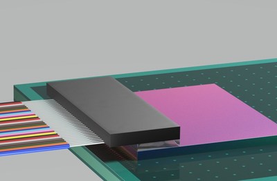
Teramount PhotonicPlug assembled on silicon photonic chip that is processed with wafer level optics
The need for high-speed data transfers in data centers, telecom networks, sensors and emerging applications in advanced computing for artificial intelligence (AI) is growing exponentially. This in turn is driving the importance of developing solutions that can cost-effectively scale up production of silicon photonics, which enable ultra-high bandwidth performance. The collaboration between EVG and Teramount aims to solve this problem.
"Our joint work with EVG has been very successful in producing this innovative synergy between wafer-level optics and silicon photonics wafer manufacturing," said Hesham Taha, CEO of Teramount. "By offering this capability to the industry, Teramount solves one of the major hurdles to further adoption of optical connectivity, which is critical for so many applications that require high-speed data transfers and low power consumption."
"Teramount's PhotonicPlug silicon photonics packaging technology is a truly novel approach to improving optical performance, and we are excited to be a partner in helping to bring it to the market," stated Markus Wimplinger, Corporate Technology Development and IP Director at EV Group. "This is just the latest example of innovative technology developed with the support of EVG's process and equipment know-how through our NILPhotonics Competence Center, where we help our partners and customers turn new ideas into innovative products."


