
First scalable integrated laser and microcomb on one chip
UC Santa Barbara team announce laser breakthrough
Fifteen years ago, UC Santa Barbara electrical and materials professor John Bowers pioneered a method for integrating a laser onto a silicon wafer. The technology has since been widely deployed in combination with other silicon photonics devices to replace the copper-wire interconnects that formerly linked servers at data centres, dramatically increasing energy efficiency - an important endeavour at a time when data traffic is growing by roughly 25 percent per year.
For several years, the Bowers group has collaborated with the group of Tobias J. Kippenberg at the Swiss Federal Institute of Technology (EPFL), within the Defense Advanced Research Projects Agency (DARPA) Direct On-Chip Digital Optical Synthesiser (DODOS) program. The Kippenberg group discovered 'microcombs', a series of parallel, low-noise, highly stable laser lines. Each of the many lines of the laser comb can carry information, extensively multiplying the amount of data that can be sent by a single laser.
Recently, several teams demonstrated very compact combs by placing a semiconductor laser chip and a separate silicon nitride ring-resonator chip very close together. However, the laser and the resonator were still separate devices, made independently and then placed in close proximity to each other perfectly aligned, a costly and time-consuming process that is not scalable.
The Bowers lab has worked with the Kippenberg lab to develop an integrated on-chip semiconductor laser and resonator capable of producing a laser microcomb. A paper titled 'Laser soliton microcombs heterogeneously integrated on silicon' published in the new issue of the journal Science, describes the labs' success in becoming the first to achieve that goal.
Soliton microcombs are optical frequency combs that emit mutually coherent laser lines -- that is, lines that are in constant, unchanging phase relative to each other. The technology is applied in the areas of optical timing, metrology and sensing. Recent field demonstrations include multi-terabit-per-second optical communications, ultrafast LiDAR, neuromorphic computing, and astrophysical spectrometer calibration for planet searching, to name several. It is a powerful tool that normally requires exceptionally high power and expensive lasers and sophisticated optical coupling to function.
The working principle of a laser microcomb, explained lead author Chao Xiang, a postdoctoral researcher in Bowers's lab, is that a distributed feedback (DFB) laser produces one laser line. That line then passes through an optical phase controller and enters the micro-ring resonator, causing the power intensity to increase as the light travels around the ring. If the intensity reaches a certain threshold, non-linear optical effects occur, causing the one laser line to create two additional, identical lines on either side. Each of those two "side lines" creates others, leading to a cascade of laser-line generation. "You end up with a series of mutually coherent frequency combs," Xiang said - and a vastly expanded ability to transmit data.
This research enables semiconductor lasers to be seamlessly integrated with low-loss nonlinear optical micro-resonators - "low-loss" because the light can travel in the waveguide without losing a significant amount of its intensity over distance. No optical coupling is required, and the device is entirely electrically controlled. Importantly, the new technology lends itself to commercial-scale production, because thousands of devices can be made from a single wafer using industry standard CMOS-compatible techniques. "Our approach paves the way for large-volume, low-cost manufacturing of chip-based frequency combs for next-generation high-capacity transceivers, data centres, space and mobile platforms," the researchers stated.
The key challenge in making the device was that the semiconductor laser and the resonator, which generates the comb, had to be built on different material platforms. The lasers can be made only with materials from the III and V groups on the Periodic Table, such as indium phosphide, and the best combs can be made only from silicon nitride. "So, we had to find a way to put them together on a single wafer," Xiang explained.
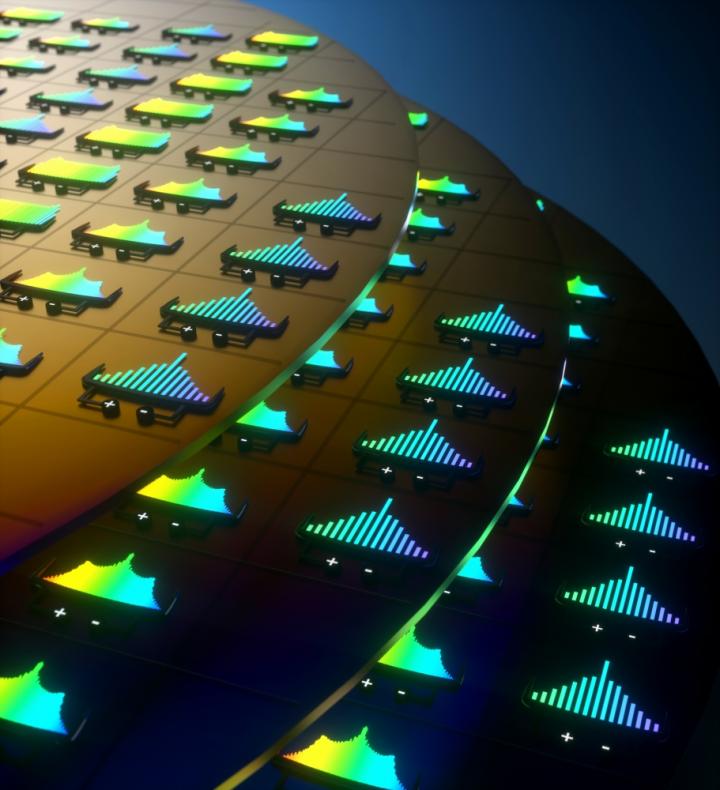
Working sequentially on the same wafer, the researchers leveraged UCSB's heterogeneous integration process for making high-performance lasers on silicon substrate and the ability of their EPFL collaborators to make record ultra-low-loss high-Q silicon nitride micro-resonators using the "photonic damascene process" they developed. The wafer-scale process -- in contrast to making individual devices and then combining them one by one -- enables thousands of devices to be made from a single 100-mm-diameter wafer, a production level that can be scaled up further from the industry standard 200-mm- or 300-mm-diameter substrate.
For the device to function properly, the laser, the resonator and the optical phase between them must be controlled to create a coupled system based on the "self-injection locking" phenomenon. Xiang explained that the laser output is partially back-reflected by the micro-resonator. When a certain phase condition is achieved between the light from the laser and the back-reflected light from the resonator, the laser is said to be locked to the resonator.
Normally, back-reflected light harms laser performance, but here it is crucial for generating the microcomb. The locked laser light triggers soliton formation in the resonator and reduces the laser light noise, or frequency instability, at the same time. Thus, something harmful is transformed into a benefit. As a result, the team was able to create not only the first laser soliton microcomb integrated on a single chip, but also the first narrow-linewidth laser sources with multiple available channels on one chip.
"The field of optical comb generation is very exciting and moving very fast. It is finding applications in optical clocks, high-capacity optical networks and many spectroscopic applications," said Bowers, the Fred Kavli Chair in Nanotechnology and the director of the College of Engineering's Institute for Energy Efficiency. "The missing element has been a self-contained chip that includes both the pump laser and the optical resonator. We demonstrated that key element, which should open up rapid adoption of this technology."
"I think this work is going to become very big," said Xiang. The potential of this new technology, he added, reminds him of the way putting lasers on silicon 15 years ago advanced both research and industrial commercialisation of silicon photonics. "That transformative technology has been commercialised, and Intel ships millions of transceiver products per year," he said. "Future silicon photonics using co-packaged optics will likely be a strong driver for higher-capacity transceivers using a large number of optical channels."
Xiang explained that the current comb produces about twenty to thirty usable comb lines and that the goal going forward will be to increase that number, "hopefully to get one hundred combined lines from each laser-resonator, with low power consumption."
Based on the soliton microcombs' low energy use and their ability to provide a large number of high-purity optical comb lines for data communications, said Xiang, "We believe that our achievement could become the backbone of efforts to apply optical frequency comb technologies in many areas, including efforts to keep up with fast-growing data traffic and, hopefully, slow the growth of energy consumption in mega-scale data centres."


