Imec Joins Forces With Sivers Photonics and ASM AMICRA
imec, a leading research and innovation center in nanoelectronics and digital technologies, together with Sivers Photonics (formerly CST Global, and a subsidiary of Sivers Semiconductors), a UK-based high-volume manufacturer of III-V compound semiconductors for photonics products, and ASM AMICRA Microtechnologies, a worldwide leading supplier of ultra-high precision die attach equipment, announce the successful wafer-scale integration of indium-phosphide (InP) distributed feedback
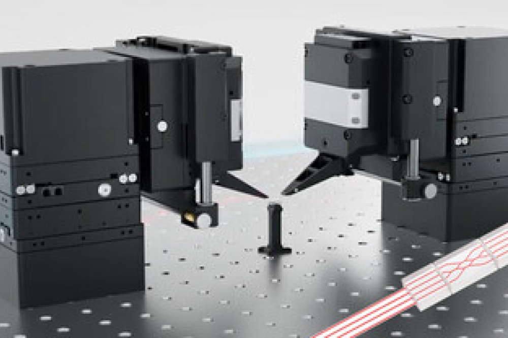
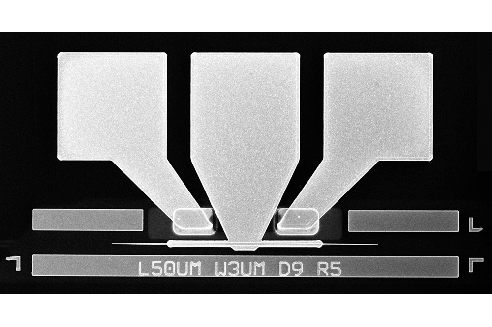
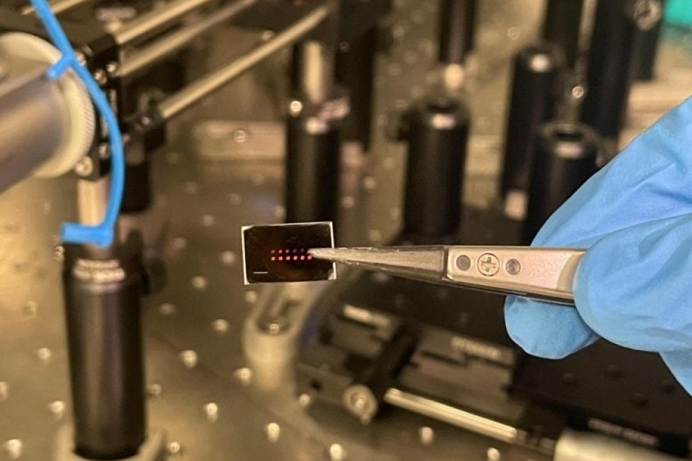
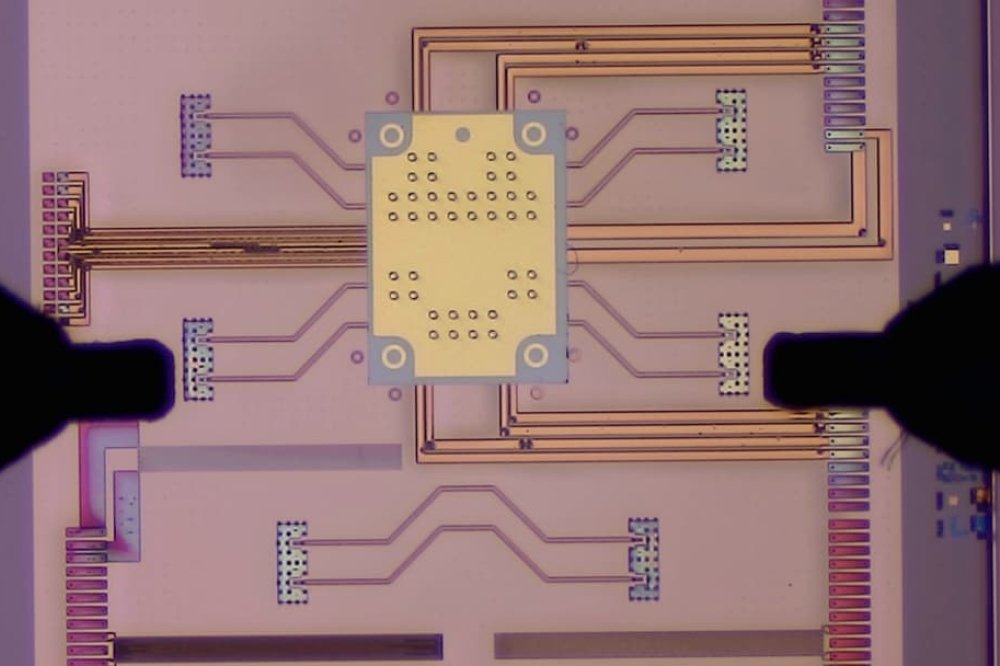
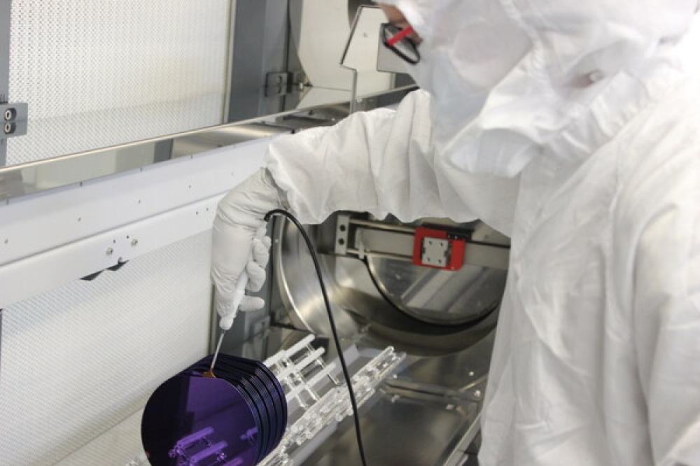
(DFB) lasers from Sivers’ InP100 platform onto imec’s silicon photonics platform (iSiPP). Using ASM AMICRA’s latest NANO flip-chip bonder tool, the InP DFB laser diodes were bonded onto a 300mm silicon photonics wafer with an alignment precision within 500nm, enabling reproducible coupling of more than 10mW of laser power into the silicon nitride waveguides on the silicon photonics wafer. Supported by its partners, imec will offer this technology later in 2021 as a prototyping service, thereby accelerating the adoption of silicon photonics in a wide range of applications from optical interconnects, over LiDAR, to biomedical sensing.
Many silicon photonic systems today still rely on external light sources, owing to the lack of efficient on‐chip light sources. Silicon itself does not emit light efficiently and, therefore, light sources made of III-V semiconductors, such as indium-phosphide (InP) or gallium-arsenide (GaAs), are typically implemented as separately packaged components. However, these off‐chip lasers often suffer from higher coupling losses, a large physical footprint and a high packaging cost.
Together with its partners Sivers and ASM AMICRA, imec is extending its silicon photonics prototyping services to include high-precision flip-chip integration capability of InP lasers and amplifiers. In the recently completed development phase, C-band InP DFB lasers have been passively aligned and flip-chip bonded onto 300mm silicon photonics wafers with ultra-high alignment precision within 500nm (three-sigma value), resulting in reproducible on-chip waveguide-coupled laser power beyond 10mW. Throughout the second half of 2021, the hybrid integration portfolio will be extended with reflective semiconductor optical amplifiers (RSOA), leveraging the etched-facet capability of Sivers’
InP100 technology, and ASM AMICRA NANO’s superior bonding alignment precision. This capability will enable advanced, external cavity laser source types, as required for emerging optical interconnect and sensing applications, and will become available in early 2022.
Joris van Campenhout, Optical I/O Program Director at imec: “We are very pleased to be working with Sivers Photonics and ASM AMICRA to extend our silicon photonics platform with hybrid integrated laser sources and amplifiers. This additional functionality will enable our joint customers to develop and prototype advanced photonic integrated circuits
(PICs) with capabilities well beyond what we can offer today, in key areas such as datacom, telecom and sensing.”
Billy McLaughlin, Sivers Photonics Managing Director: “We’re excited to work with imec and ASM AMICRA on the development of advanced integrated photonic components. The availability of InP laser sources, designed and fabricated on our InP100 manufacturing platform, will boost the adoption of silicon photonic circuits for a wide variety of commercial applications.”
Dr. Johann Weinhändler, ASM AMICRA Managing Director: “Our strength in high-precision placement seamlessly complements the expertise of all partners. With automated and ultra-precise flip-chip bonding, the way to high-volume manufacturing of these hybrid assemblies is open.”


