
VLC Photonics invests in Wafer-level Test system
FiconTEC's WLT system adds to portfolio of tools for PIC characterisation and testing
In order to support the growth of the Photonic Integrated Circuit (PIC) market and be able to timely serve the scaling of its customers when moving to engineering and pilot production stages, VLC Photonics is now one of a growing list of established PIC eco-system innovators to receive one of FiconTEC‘s new Wafer-level Test (WLT) systems.
The WLT delivered to VLC incorporates dual alignment of optical pick-ups that can be fast-actively aligned to optical I/O ports at on-wafer PIC devices. The addition of this system to their in-house portfolio of equipment and tools for PIC characterization and testing will complement the services offered up to now on a die level.
VLC Photonics, based in Valencia, Spain, is a fabless photonic design house, recently part of the Hitachi High-Tech group, offering varying services for organizations seeking to exploit the advantages of photonic integration. These services nowadays cover all aspects of PIC development, from initial consultancy to design, manufacturing, test, and packaging. For this purpose, VLC has continually grown a global portfolio of customers and additionally partnered with renowned foundries and packagers to successfully serve a broad spectrum of applications in communications, sensing, quantum optics, biophotonics, instrumentation and other sectors.
Just as for its other services, the new WLT capability can be offered for a comprehensive range of on-wafer component types, irrespective of the material system. This includes integrated photonics-enabled elements and devices based on the SOI, SiN and InP material systems, as well as components based on planar lightwave circuits (PLC). The component size can lie anywhere in the range from 2x2 to 20x20 mm², while the wafer-handling system present in the WLT is compatible with single dies and wafer sizes from 3 inches up to 12 inches.
Iñigo Artundo, CEO at VLC Photonics, foresees particular benefits emerging through the addition of the WLT system: “Back-end packaging and test has always been acknowledged to be the main bottleneck when industrialising PIC-based products, and most of our developments and acquisitions in recent years are designed to help our customers succeed in facing the challenges associated with PIC testing.”
Torsten Vahrenkamp, CEO at FiconTEC said: “We have worked intensively on our WLT capability over the last two years, and we are really excited to see this technology finding acceptance amongst commercial PIC service sector leaders such as VLC Photonics. Notwithstanding, this is just a momentary snapshot of where we are going with the WLT systems, and we are continuing to collaborate with leading partners in specific technology areas to provide efficient mixed-signal electro-optical testing and high-volume capability in the near-term”.
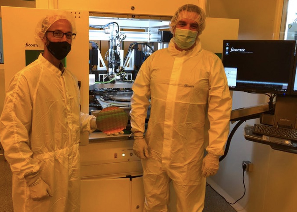
The WLT tool was received in November 2020 and it is now in production at the facilities of VLC Photonics in the UPVfab cleanroom.
The piicture above shows VLC Photonics’ CTO David Domenech and FiconTEC production engineer Tim Kluge after installation of the new WLT system.


