Aehr Receives Multi-Wafer Test & Burn-in Solution Order

Aehr Test Systems, a worldwide supplier of semiconductor test and reliability qualification equipment, has announced it has received an order totaling over $1.4 million from an existing customer for a FOX-XPTM multi-wafer test and burn-in system and multiple WaferPak Contactors to perform volume production qualification of the customers’ high performance silicon photonics devices. The total FOX solution is expected to ship prior to the end of Aehr’s current fiscal year ending May 31, 2021.
Gayn Erickson, President and CEO of Aehr Test Systems, commented, “This customer is a major supplier of fiber optic transceivers in the Data Center Interconnect (DCI) market and is moving to silicon photonics integration to address higher performance and lower cost needs of the market. We are delighted to see them transition from our FOX-NP™ system for initial production burn-in and stabilization of their high-performance silicon photonic devices to using our production FOX-XP system to meet their high-volume production forecast. The DCI market includes DCI-Long Haul from city to city, DCI-Metro from Data Center to Data Center within a city, and DCI-Campus/Edge for high bandwidth transmission between multiple data centers within a campus or used to connect regional, distributed data centers. The five year cumulative average growth rate (CAGR) of the DCI market is expected to grow at over 55% from 2019 to 2023 alone according to Cignal AI. This is now our sixth customer in the silicon photonics space that is using our FOX platform for qualification and production.
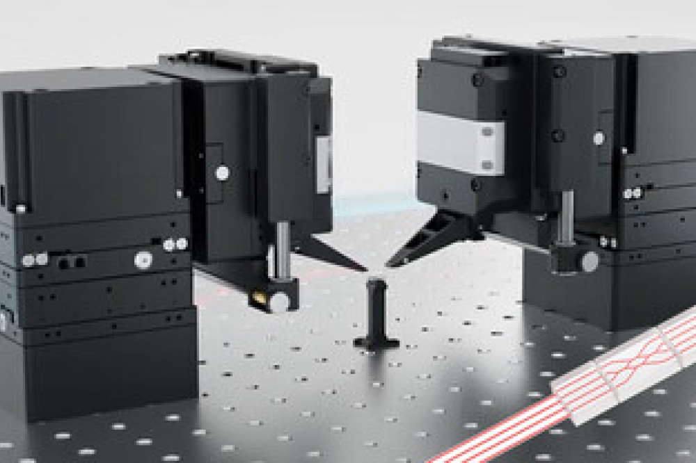
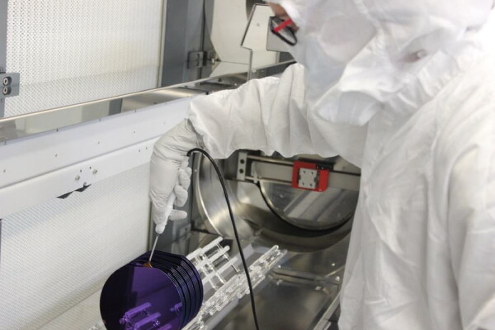
“This is a 100% production test application, so unlike a sampling burn-in process step, this customer is using the FOX system to stabilize each device as a critical production process step, and will need incremental capacity for FOX systems and WaferPaks with each increment in their volume production forecast. Our high volume, high power production FOX-XP system is capable of testing up to 9 high-power wafers in parallel to meet their production needs. With up to 2,000 watts of power per wafer, and the ability to test thousands of individual devices in parallel with our WaferPak full wafer contactor, the FOX-XP solution can test all devices on each wafer in parallel in a single touchdown. The FOX-XP is 100% compatible with our dual-wafer FOX-NP and proprietary WaferPaks, which allow our customers to make a very simple transition between initial qualification and low volume production to high volume production.
“We are excited to see this new wave of capacity needs from our silicon photonics customers, and to see the resumption of orders to these customers for devices for data center and 5G infrastructure expansions that is driving the increased test capacity need. We continue to be very optimistic about the silicon photonics market, which is seeing increasing deployment of devices used in the expansion of bandwidth and infrastructure to meet the explosive growth of data center and 5G. Silicon photonics devices are highly integrated silicon based semiconductors that have embedded or integrated the non-silicon based laser transmitters and receivers to enable a smaller, lower cost, higher reliable alternative to traditional fiber optic transceivers currently used in data center and telecommunication infrastructure.
“Silicon photonics devices all need to have their photonics transmitters stabilized under high power and temperature and customers also use our systems to screen for infant mortality of these devices to ensure high initial quality and long-term reliability. This is a manufacturing step done on 100% of the die, and in the case of silicon photonics we provide a much more cost effective and scalable solution for this step than doing this equivalent stabilization and screening after the die are put onto the final PCB substrate and package. Market research company Yole Dévelopement predicts the silicon photonics market will grow at a CAGR of 42% between 2019 and 2025 to a $3.6 billion annual market and we believe that the industry will transition to wafer level or singulated die for this critical manufacturing step, which is where our FOX-P products stand alone as the most cost-effective solution for this on the market”
The semiconductor industry today exceeds $400 billion per year with a single CMOS chip containing billions of transistors, forming complex circuits that are still 100% electrical. Using photons instead of electrons, silicon photonics brings optical communications into the fabrication space of the semiconductor industry, enabling low-cost, high-volume assembly and the capability to bring faster, smaller, interconnects, which consume less power and offer the entire semiconductor industry a whole new world of opportunities. Silicon photonics is expected to be the most scalable optical transceiver technology available while delivering lowest cost per bit for 100Gb and higher transfer speeds. Next generation data centers, high performance computers, and eventually consumer video products will all benefit from optical interconnects built from silicon photonics.
The FOX-XP system, available with multiple WaferPak™ Contactors (full wafer test) or multiple DiePak™ Carriers (singulated die/module test) configurations, is capable of functional test and burn-in/cycling of integrated devices such as silicon carbide power devices, silicon photonics as well as other optical devices, 2D and 3D sensors, flash memories, Gallium Nitride (GaN), magnetic sensors, microcontrollers, and other leading-edge ICs in either wafer formfactor, before they are assembled into single or multi-die stacked packages, or in singulated die or module formfactor.


