II-VI Unveils VCSEL Arrays for next gen 3D sensing

Double-junction 940nm technology doubles the power output per VCSEL emitter and improves the power conversion efficiency to 56 percent
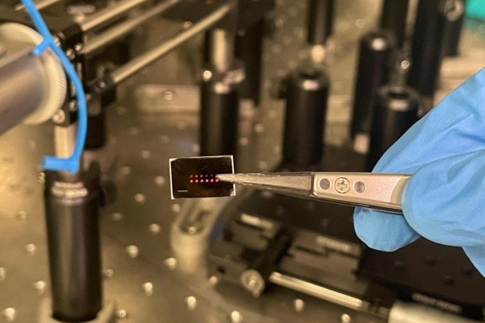
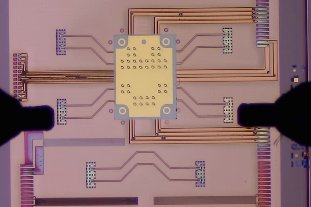
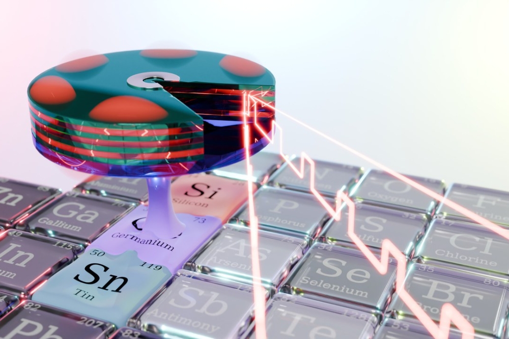
II-VI has announced its double-junction VCSEL arrays, the first of its multi-junction VCSEL array platforms for next-generation world-facing 3D sensing applications.
The growing adoption of 3D sensing in several markets, including in consumer electronics, automotive, and industrial, is driving the demand for depth sensors with longer and wider range, lower power consumption, smaller size, and lower cost.
II-VI˙s new VCSEL arrays are based on a double-junction technology that doubles the power output per VCSEL emitter and improves the power conversion efficiency to 56 percent, compared with 46 percent in existing single-junction technology. This can be leveraged for a number of differentiating benefits, including higher output power to sense farther and wider, reduced battery power consumption, and smaller size to achieve lower cost and to enable more inconspicuous designs.
"We have developed over the years strong partnerships with our customers, closely collaborating on the development of long-term technology and product roadmaps aimed at providing breakthrough solutions and continuously elevating user experience in 3D sensing," said Julie Eng, SVP, Optoelectronic & RF Devices Business Unit.
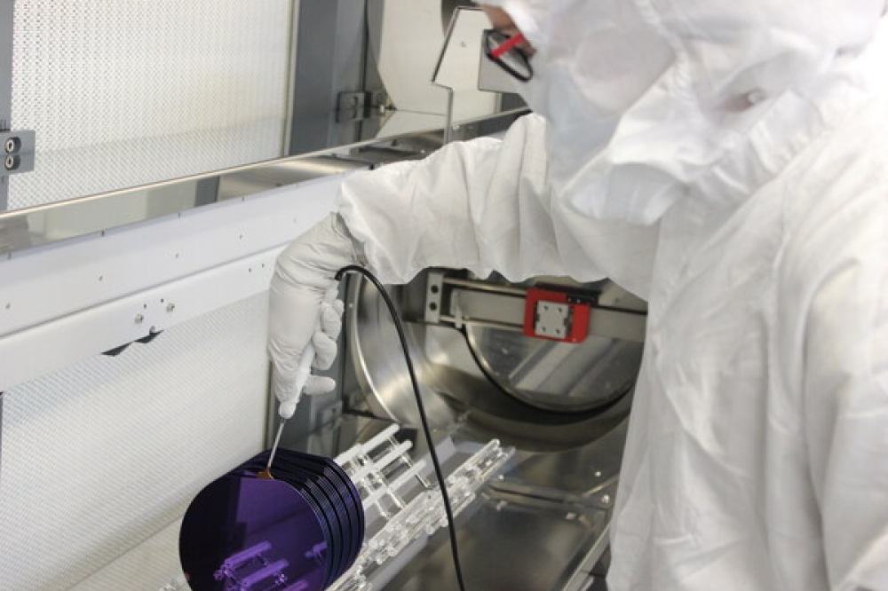
"A few years ago, we successfully scaled our vertically integrated GaAs optoelectronics technology platform from 3-inch to 6-inch, which enabled us to shorten our development cycles and introduce new products to meet aggressive market windows. We are now once again evolving the platform, this time with a leap to double-junction technology that we believe will unlock exciting new use cases, such as farther depth of sensing in world-facing applications and seamless integration into consumer products for AR and VR applications."
II-VI˙s double-junction VCSEL arrays emit at 940 nm, and their steep slope efficiencies enable very short pulses of very high peak powers. The VCSEL arrays are designed for low-cost non-hermetic packaging and, like the single-junction arrays, can be reliably and cost-effectively scaled in total power by increasing the number of emitters per chip. They can also be produced in high volume on II-VI˙s vertically integrated 6-inch platform.
II-VI˙s broad portfolio of products for 3D sensing includes diffractive optical elements (DOEs) and thin-film filters that are produced at wafer-scale for high-volume applications. DOE flat lenses and lenslet arrays collimate, focus, or transform beams from VCSEL arrays. DOE diffusers homogenize the output of VCSEL arrays and produce a uniform field of illumination. DOE splitters separate an input beam into multiple output beams. Filters are used to improve the signal-to-noise ratio of the image sensor array. II-VI VCSEL arrays are available as chips or integrated with DOEs in surface-mount technology packages.
II-VI will show its line of lasers and optics for 3D sensing at the 2021 SPIE Photonics West Digital Forum, March 6-11, 2021.


