
EV Group establishes state-of-the-art customer training facility
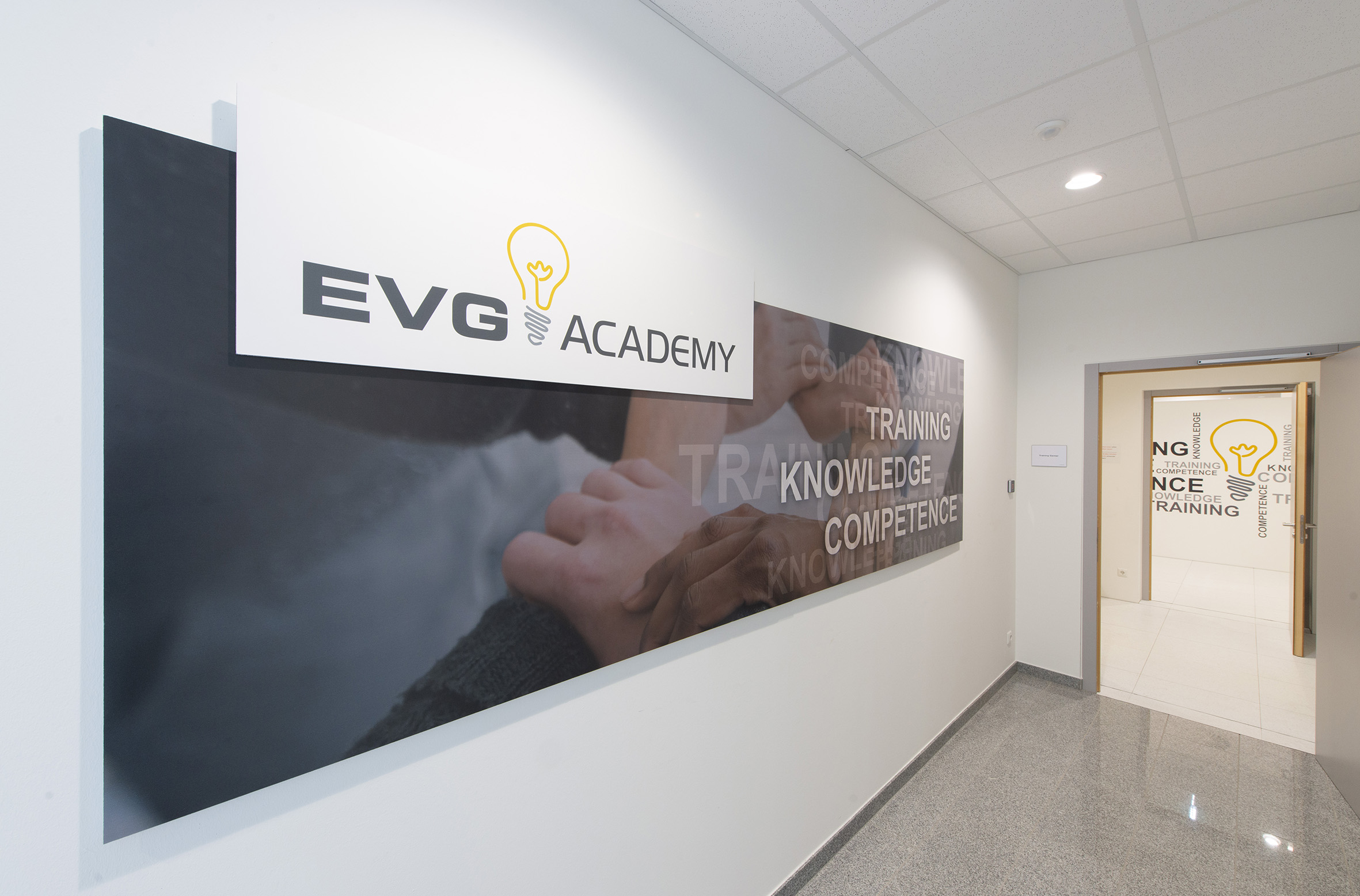
EV Group (EVG), a supplier of wafer bonding and lithography equipment for the MEMS, nanotechnology, and semiconductor markets, has announced that it has established the EVG Academy, a training facility for customers that provides technical training on all classes of EVG equipment as well as on EVG's CIM Framework software platform in an optimized environment. Established at EVG's headquarters in Austria, the EVG Academy comprises a new 800-square-meter facility created in tandem with the recently completed Cleanroom V expansion project. By attending in-depth, tiered training classes at the EVG Academy, customers can be qualified to perform basic repairs as well as preventative maintenance on EVG equipment without the need to contact EVG customer support -- providing customers with greater flexibility for tool maintenance. The new training facility also serves as the education and training hub for EVG's global organization.
The EVG Academy builds on EVG's existing training facilities at its headquarters, doubling the amount of training space and technical trainers. It includes eight individual training areas -- one for each major class of EVG equipment -- as well as four classrooms and a dedicated workshop area for electrical and mechanical training. Thanks to the additional floorspace, the EVG Academy has also expanded the number and type of tools available for training, including EVG's fully automated HVM platforms, such as the GEMINI® FB automated production wafer bonding system with SmartView® NT3 bond aligner and the BONDSCALE® automated production fusion bonding system.

"The EVG Academy was purpose-built with the goal to enable in-depth customer training on all EVG platforms utilizing the latest equipment and technologies, including our most advanced fully automated high-volume manufacturing (HVM) tools," stated Helmut Pfeifer, vice president of customer support. "EVG has made significant investments in updating our training infrastructure, and we are extremely proud of this world-class facility, which sets new standards for knowledge transfer in our industry. The new EVG Academy will greatly enhance the learning experience for both our customers and our international customer support teams."
The EVG Academy builds on EVG's existing training facilities at its headquarters, doubling the amount of training space and technical trainers. It includes eight individual training areas -- one for each major class of EVG equipment -- as well as four classrooms and a dedicated workshop area for electrical and mechanical training. Thanks to the additional floorspace, the EVG Academy has also expanded the number and type of tools available for training, including EVG's fully automated HVM platforms, such as the GEMINI® FB automated production wafer bonding system with SmartView® NT3 bond aligner and the BONDSCALE® automated production fusion bonding system.
The EVG Academy is now open for training. Customers interested in learning more can contact EVG at academy@evgroup.com.


