+44 (0)24 7671 8970
More publications     •     Advertise with us     •     Contact us
 
Loading...
News Article

ACM Research Enters 3D TSV Copper Plating Market

News

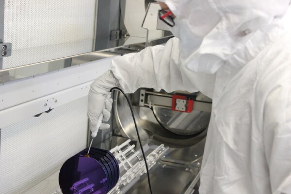
ACM Research, a supplier of wafer processing solutions for semiconductor and advanced wafer-level packaging (WLP) applications, today introduced its Ultra ECP 3d platform for conformally filled 3D through-silicon via (TSV) applications. Leveraging ACM’s Ultra ECP ap and map platforms, the Ultra ECP 3d platform delivers high-performance copper (Cu) electroplating for high aspect ratio (HAR) Cu applications, with no voids or seams. Key markets for devices using TSVs include imaging, memory, MEMS and optoelectronics, among others.

According to industry research firm Mordor Intelligence, “The 3D TSV Devices Market was valued at USD $2.8 billion in 2019 and is expected to reach USD $4.0 billion by 2025, at a CAGR of 6.2% over the forecast period of 2020 - 2025.”

“Many factors are driving the growth of the 3D TSV market, from device miniaturization to AI and edge computing,” said David Wang, CEO of ACM. “These applications demand more processing power in ever higher density packages and are leading to rapid industry adoption of TSV technologies.”

“In working with customers, we’ve successfully demonstrated our ability to fill HAR vias using the Ultra ECP 3d platform. In addition to delivering higher throughput with a stacked chamber design, the platform is designed to use fewer consumables, have a lower total cost of ownership, and save valuable fab floor space,” Wang added.

During bottom-up filling for HAR TSVs, the Cu electrolyte must be able to completely fill the vias without any trapped air bubbles when immersed in the plating solution. To accelerate this process, an integrated pre-wet step is used.

This advanced technology solution can deliver better yields, greater plating efficiency and higher throughput during the fabrication process. The Ultra ECP 3d platform for 3D TSV is a 10-chamber, 300mm tool with integrated pre-wet, Cu plating and post-clean modules in a footprint of only 2.20m x 3.60m x 2.90m (W/L/H).

ACM recently delivered its first Ultra ECP 3d tool to a key customer in China, to begin formal qualification for its 3D TSV and 2.5D interposer Cu plating applications. For more information, please call the ACM regional company contact listed below.

EMCORE announces integration of PICs into its products
Scottish photonics consortium wins £4.7m in UKRI funding
Yuanjie Semiconductor to supply lasers to POET
Fraunhofer IPMS announces government funding for quantum photonic chip
POET Technologies partners with Yuanjie Semiconductor Technology
SiLC announces silicon photonics systems for machine vision
Scientists develop novel optical modulators for integrated photonics
Scientists report integrated photodiodes on TFLN
Coherent wins award for innovative photonics product
FBH to present quantum technology developments at EQTC 2023
Skorpios and FormericaOE demonstrate PICs in 800G optical transceivers
EFFECT Photonics verifies fully integrated InP PIC
NASA awards grant for silicon photonics project
OpenLight and Spark Photonics partner on PIC design services
DustPhotonics announces 800G chip for hyperscale data centres and AI
Lightwave Logic Receives Industry Innovation Award
Imec announces SiGe BiCMOS optical receiver
SiFotonics announces silicon photonics 800G LPO solutions
Rockley Photonics progresses noninvasive biomarker monitoring
MantiSpectra secures €4 million for miniaturised spectrometers
Sivers to demo next-gen laser arrays at ECOC 2023
ASMPT AMICRA and Teramount collaborate on silicon photonics packaging
Quantum Computing Inc. selects Arizona site for photonic chip foundry
German government to fund ams OSRAM optoelectronic semiconductor development
Luceda Photonics introduces new PIC design software
Vodafone explores silicon photonics for future mobile networks
Coherent introduces 1200 mW pump laser module
Photonics startups invited to apply to Luminate NY accelerator
New tool could improve lithography for smaller, faster chips
InP-based lasers surpass 2.2 mm
Indie Semiconductor buys Exalos AG
New technique controls direction and wavelength of emitted heat

×
Search the news archive

To close this popup you can press escape or click the close icon.
Logo
×
Logo
×
Register - Step 1

You may choose to subscribe to the PIC Magazine, the PIC Newsletter, or both. You may also request additional information if required, before submitting your application.


Please subscribe me to:


You chose the industry type of "Other"

Please enter the industry that you work in: