+44 (0)24 7671 8970
More publications     •     Advertise with us     •     Contact us
 
Loading...
News Article

Hamamatsu Photonics announces the completion of a new factory building at the Shingai factory site.

News

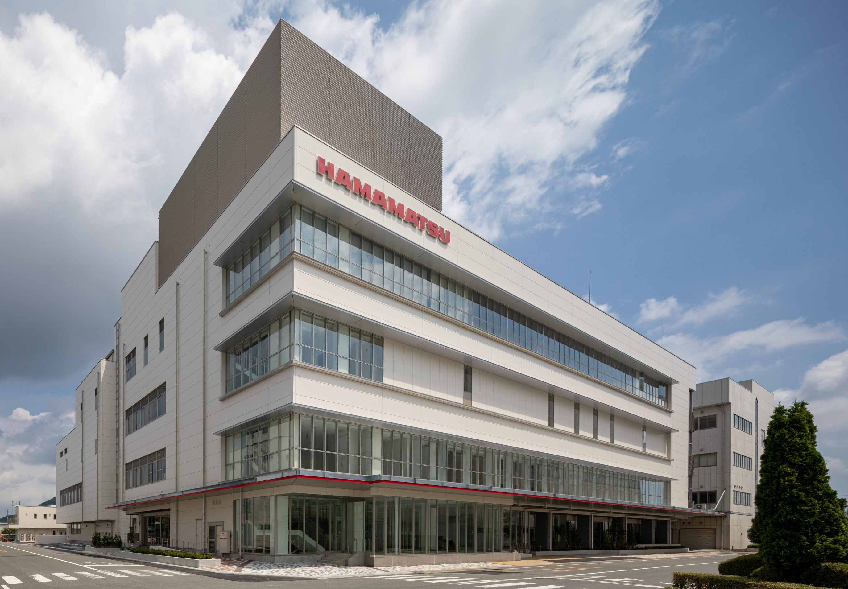
Hamamatsu Photonics has been constructing a new factory building at the Shingai Factory (Shingai-cho, Minami-ku, Hamamatsu City, Japan) to cope with increasing sales demand for opto-semiconductors, X-ray image sensors and X-ray flat panel sensors. This new factory will start operations in October this year. The completion ceremony for the new factory building took place Friday, August 7.

Hamamatsu Photonics has been supplying opto-semiconductor products for a wide range of applications and fields such as medical diagnosis and treatment, industrial instrumentation, automotive, and scientific measurement. Recently, there has been an increasing demand for plastic-molded opto-semiconductors mass-producible in large quantities, as well as for X-ray image sensors and X-ray flat panel sensors used in radiation inspection devices. We expect a further increase in sales of these products over a diverse spectrum of fields.

Construction of this new factory building will help us build up our production system for opto-semiconductors, X-ray image sensors, and X-ray flat panel sensors. This will also consolidate our opto-semiconductor production processes that are currently located separately from each other at the Shingai Factory and associated companies. These production processes will now all take place in the new factory building where we can streamline production efficiency and create a more robust supply system through labor-saving and automation. To boost X-ray image sensor and X-ray flat panel sensor production, we will speed up product development by consolidating design, development and evaluation into a single area and will also streamline our supply system by way of production processes located on the same floor to respond to growing demand.

To ensure business continuity against natural disasters, which have increased in recent years, we have made our anti-disaster measures more robust by incorporating earthquake and flood control measures into the building structure of the new factory. At the same time, the new factory building is designed to actively incorporate eco-friendly measures such as LED lighting, heat-insulated walls, solar power plant, and rainwater reuse systems.

EMCORE announces integration of PICs into its products
Scottish photonics consortium wins £4.7m in UKRI funding
Yuanjie Semiconductor to supply lasers to POET
Fraunhofer IPMS announces government funding for quantum photonic chip
POET Technologies partners with Yuanjie Semiconductor Technology
SiLC announces silicon photonics systems for machine vision
Scientists develop novel optical modulators for integrated photonics
Scientists report integrated photodiodes on TFLN
Coherent wins award for innovative photonics product
FBH to present quantum technology developments at EQTC 2023
Skorpios and FormericaOE demonstrate PICs in 800G optical transceivers
EFFECT Photonics verifies fully integrated InP PIC
NASA awards grant for silicon photonics project
OpenLight and Spark Photonics partner on PIC design services
DustPhotonics announces 800G chip for hyperscale data centres and AI
Lightwave Logic Receives Industry Innovation Award
Imec announces SiGe BiCMOS optical receiver
SiFotonics announces silicon photonics 800G LPO solutions
Rockley Photonics progresses noninvasive biomarker monitoring
MantiSpectra secures €4 million for miniaturised spectrometers
Sivers to demo next-gen laser arrays at ECOC 2023
ASMPT AMICRA and Teramount collaborate on silicon photonics packaging
Quantum Computing Inc. selects Arizona site for photonic chip foundry
German government to fund ams OSRAM optoelectronic semiconductor development
Luceda Photonics introduces new PIC design software
Vodafone explores silicon photonics for future mobile networks
Coherent introduces 1200 mW pump laser module
Photonics startups invited to apply to Luminate NY accelerator
New tool could improve lithography for smaller, faster chips
InP-based lasers surpass 2.2 mm
Indie Semiconductor buys Exalos AG
New technique controls direction and wavelength of emitted heat

×
Search the news archive

To close this popup you can press escape or click the close icon.
Logo
×
Logo
×
Register - Step 1

You may choose to subscribe to the PIC Magazine, the PIC Newsletter, or both. You may also request additional information if required, before submitting your application.


Please subscribe me to:


You chose the industry type of "Other"

Please enter the industry that you work in: