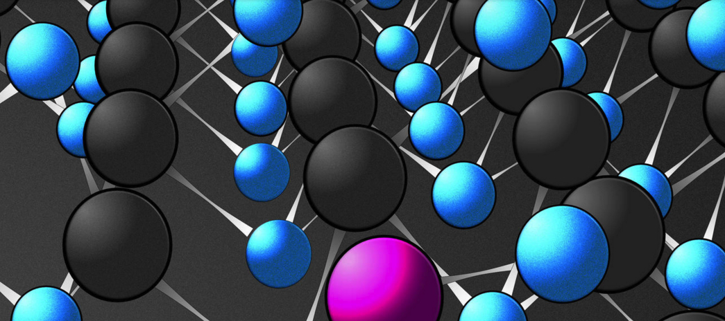
Deciphering 2D disorder
US researchers quantify disorder in 2D materials to build better quantum, optical and electronic devices
The next wave of quantum, optical and electronic devices will be built from powerful two-dimensional materials. These materials can host room temperature qubits thereby enabling solid-state quantum technologies that are inherently more powerful than their classical counterparts.
But, they have a weakness. Unlike 3D systems, where almost all of the atoms are protected from the environment, 2D materials are exposed to the elements and susceptible to outside interactions from nearby materials or chemicals in the air. These interactions can actually change the atomic arrangement of the system.
If researchers are going to build new devices out of 2D materials, they need to understand where their atoms are and how tiny imperfections change their material and electronic properties.
Researchers at the Harvard John A. Paulson School of Engineering and Applied Sciences (SEAS), the University of California, Los Angeles, and the Oak Ridge National Laboratory have combined experimental and theoretical techniques to measure atomic positions of all the atoms in a 2D transition metal dichalcogenide material and to calculate how the arrangement impacts the electronic properties of various regions of the system.
The research is published in Nature Materials.
The researchers found that materials were far from perfect, with atoms constantly misaligned, missing, or replaced with something else.
"While it makes sense that missing atoms and substituted atoms would change the local interactions and atomic configuration, it's not easy to answer the question by how much," said Christopher Ciccarino, a graduate student in the NarangLab at SEAS and co-author of the paper.
In collaboration with John Miao, professor at UCLA's Department of Physics and Astronomy, the researchers used a high-powered scanning electron microscope to measure the precise location of individual atoms and image atomic configurations at different angles relative to the 2D sheet.
After mapping out these positions, the research team analysed the lattice to see how imperfections play a role in its properties.
"Defects within the lattice created local disorder and irregularities," said Prineha Narang, Assistant Professor of Computational Materials Science at SEAS and co-author of the paper. "Even when zoomed out, the collection of vacancies and defects seemed to contribute to disorder. In particular, the 2D sheet wasn't really 2D, but instead had long range ripples in the third dimension."
"What we saw were these supposedly 2D sheets preferring to use this third dimension instead of remaining perfectly flat," said Ciccarino. "It is interesting then to think about how this would play into the observed properties of the material." The researchers found that local disorder can have significant effects on electronic and optical properties of 2D materials, including huge effects in how efficiently the material emitted light.
"Theorists usually have to make some assumptions about their system in order to compare with experiment," said Narang. "Here we were in a unique and exciting situation where we could directly intersect our methods with experimentally computed coordinates. Direct quantification of atomic disorder and interactions with environment could be an invaluable technique for fully understanding the nature and potential of these materials."
This research was funded by the Department of Defense Army Research Office MURI on Ab Initio Quantum Materials (AIQM) and the Betty and Gordon Moore Foundation. PN is a Moore Inventor Fellow. Scanning transmission electron microscopy experiments were conducted at the Center for Nanophase Materials Sciences, a Department of Energy Office of Science user facility at Oak Ridge National Laboratory.
'Correlating the three-dimensional atomic defects and electronic properties of two-dimensional transition metal dichalcogenides' by Xuezeng Tian et al; Nature Materials (2020)