
Yole forecasts growth of rear 3D sensing
Time of Flight is changing the value of the 3D sensing module
Yole Développement expects the global 3D imaging and sensing market to expand from $5.0 billion in 2019 to $15.0 billion in 2025, at a 20 percent CAGR, according to its annual imaging technology and market analysis report, '3DImaging and Sensing'.
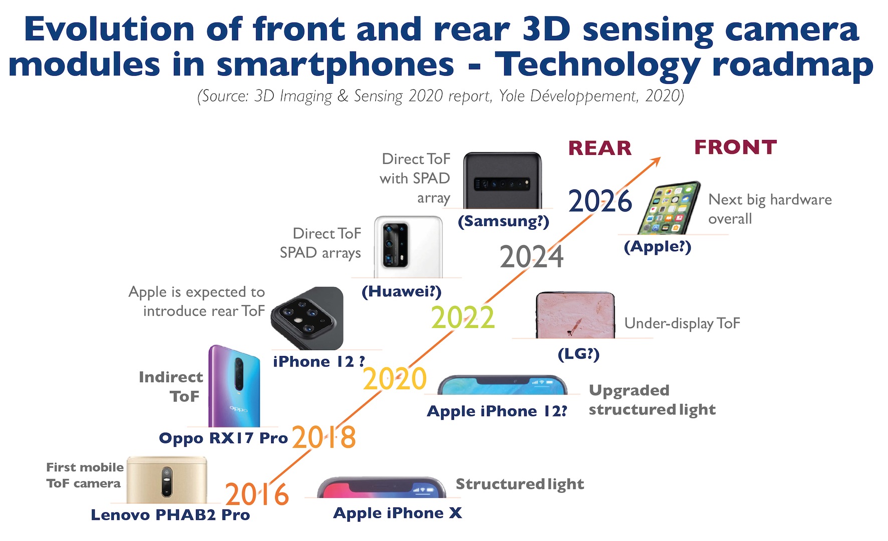
With the introduction of the iPhone X in September 2017, Apple set the technology and use-case standard for 3D sensing in the consumer space. Two years later, Android phone makers have taken a different approach, using Time of Flight (ToF) cameras instead of Structured Light and are placing them on the rear of the phone.
Richard Liu, technology and market analyst in the Photonics, Sensing & Display division at Yole and based in Shenzhen, China, adds: “Compare to structured light, ToF modules only needs a VCSEL and a diffuser on the emitter, which is less complex. ToF sensors have now improved a lot thanks to the BSI technique. They have also gained a cost advantage within a maturing ecosystem. This is the main reason why ToF has won the favor of Android phone makers”.
3D sensing's main trend is the switch from the front to the rear of phones and the ToF camera's mass adoption. According to Yole’s 3D imaging & sensing report, rear attachment will surpass front attachment with market penetration rate reaching about 42 percent in 2025.
Yole says that 3D rear sensing in mobiles should diversify its application use cases. First used for photography, it will expand into AR and gaming. Beyond smartphones, ToF camera modules have a broad application in intelligent driving, robots, smart homes, smart TVs, smart security and VR /AR. Currently, the application of ToF sensing technology in these fields is in its infancy.
The transition from imaging to sensing is happening now. AI -powered devices and robotics are gaining a better understanding of their surroundings, and developing a new level of interaction with humans. Stereo cameras for ADAS in cars are a highly anticipated application of 3D imaging and sensing technology.
“The most important component in this application, LiDAR , is now focused on by a large number of suppliers”, explains Richard Liu from Yole. “There are a wide range of LiDAR technologies to choose from, making the field as a very competitive one.”
In addition to automotive ADAS, and industrial AGVs in the logistics industry, face recognition and face payments in commercial sectors have been successful. As such, 3D sensing technology is becoming widespread. Technology providers of global shutter image sensors, VCSELs, injection-moulded and glass optics, DOEs, and semiconductor packaging are all benefiting.
What is the impact of ToF’s adoption on the supply chain?
“The mobile 3D sensing supply chain is changing rapidly,” says Pierre Cambou, principal analyst, Imaging at Yole. “As structured light technology was introduced in iPhones in 2017, companies like Lumentum, ams and ST Microelectronics won this first round. Later, Princeton Optronics (Ams) and Finisar were prepared to gain VCSEL market access, so the market did quickly become more competitive”.
In 2019, Finisar was acquired by II-VI. During this period, there were several other big mergers, such as Philips Photonics being acquired by Trumpf and Ams swallowing Osram. Trumpf and Ams are both actively moving into the Android camp's 3D camera supply chain, providing VCSELs to Samsung and Huawei respectively.
In China, another player is entering the 3D sensing ecosystem: The VCSEL output beam of the flood emitter for ToF requires no coding and is therefore easier to produce. This helped a Chinese supplier called Vertilite to join the market. They have already won orders Huawei for 3D sensing in 2019. This move was also driven by the policy of China cultivating local supply chains in the middle of the US-China trade conflict.
ToF camera technology was first applied to the Phab2 Pro smart phone in 2016, which was using pmd and Infineon's TOF array. A year before that, Sony bought SoftKinetic, a Belgian gesture-recognition company with its well-known DepthSense ToF sensing system. This move brought Sony from a zero market share position in 3D sensing receiver chips to 45 percent by the time ToF camera modules took off in 2019.
With its strong technology and supply capabilities, Sony is expected continue maintaining its leadership position in ToF. But as there has always been competition in this area of CIS chip manufacturing, competition will increase. pmd with partner Infineon recently announced a matching chip.
Yole’s analysts expect Samsung and STMicroelectronics to bring to market their own indirect ToF array sensors in 2020.
Samsung already adopted ToF technology notably in its Galaxy Note 10+. It has been analysed by System Plus Consulting, sister company of Yole in the reverse engineering and costing report, Samsung Galaxy Note 10+ 3D Time of Flight Depth Sensing Camera Module.
Competition remains intense. In the medium term Yole expects more opportunities for mergers and acquisitions as automotive LiDAR applications may come into play. There are a large number of highly competitive emerging companies. There are also a few Chinese startups, such as Hesai Technology, RoboSense, and LeiShen Intelligence. The underlying semiconductor products are the same: compact impact sensor chips, VCSEL, MEMS, wafer-level optical elements.


