
Moving Precision Communication, Metrology, Quantum Applications from Lab to Chip
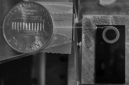
A photonic integrated circuit in which an ultralow loss 2-meter optical waveguide guiding visible light in the red spectrum is put on a silicon nitride chip smaller than a penny, important for applications such as strontium atomic clocks.
The field of photonic integration -- the area of photonics in which waveguides and devices are fabricated as an integrated system onto a flat wafer -- is relatively young compared to electronics. Photonic integration has focused on communications applications traditionally fabricated on silicon chips, because these are less expensive and more easily manufactured.
Researchers are exploring promising new waveguide platforms that provide these same benefits for applications that operate in the ultraviolet to the infrared spectrum. These platforms enable a much broader range of applications, such as spectroscopy for chemical sensing, precision metrology and computation.
A paper in APL Photonics, from AIP Publishing, provides a perspective of the field of ultra-wideband photonic waveguide platforms based on wide bandgap semiconductors. These waveguides and integrated circuits can realize power-efficient, compact solutions, and move key portions of ultra-high-performance systems to the chip scale instead of large tabletop instruments in a lab.
Until now, key components and subsystems for applications, such as atomic clocks, quantum communications and high-resolution spectroscopy, are constructed in racks and on tabletops. This has been necessary because they operate at wavelengths not accessible to silicon waveguides due to its lower bandgap and other absorption properties in the UV to near-IR that reduce the optical power handling capabilities, among other factors.
Daniel J. Blumenthal and his team in Santa Barbara, California, have researched photonic integration platforms based on waveguides fabricated with wide bandgap semiconductors that have ultralow propagation losses.
“Now that the silicon market has been addressed for telecommunications and LIDAR applications, we are exploring new materials that support an exciting variety of new applications at wavelengths not accessible to silicon waveguides,” said Blumenthal. “We found the most promising waveguide platforms to be silicon nitride, tantala (tantalum pentoxide), aluminum nitride and alumina (aluminum oxide).”
Each platform has the potential to address different applications such as silicon nitride for visible to near-IR atomic transitions, tantalum pentoxide for raman spectroscopy or aluminum oxide for UV interactions with atoms for quantum computing.
Applications, such as atomic clocks in satellites and next-generation high-capacity data center interconnects, can also benefit from putting functions such as ultralow linewidth lasers onto lightweight, low-power chips. This is an area of increased focus as exploding data center capacity pushes traditional fiber interconnects to their power and space limitations.
Blumenthal said next-generation photonic integration will require ultra-wideband photonic circuit platforms that scale from the UV to the IR and also offer a rich set of linear and nonlinear circuit functions as well as ultralow loss and high-power handling capabilities.


