
NEC develops way to speed development of new materials
Machine learning augments experimental and computational methods for cheaper predictions of material properties.
Researchers in Japan have developed an approach that can better predict the properties of materials by combining high throughput experimental and calculation data together with machine learning. The approach could help hasten the development of new materials, and was published in the journal Science and Technology of Advanced Materials.
Scientists use high throughput experimentation, involving large numbers of parallel experiments, to quickly map the relationships between the compositions, structures, and properties of materials made from varying quantities of the same elements. This helps accelerate new material development, but usually requires expensive equipment.
High throughput calculation, on the other hand, uses computational models to determine a material’s properties based on its electron density, a measure of the probability of an electron occupying an extremely small amount of space. It is faster and cheaper than the physical experiments but much less accurate.
Materials informatics expert Yuma Iwasaki of the Central Research Laboratories of NEC Corporation, together with colleagues in Japan, combined the two high-throughput methods, taking the best of both worlds, and paired them with machine learning to streamline the process.
“Our method has the potential to accurately and quickly predict material properties and thus shorten the development time for various materials,” says Iwasaki.
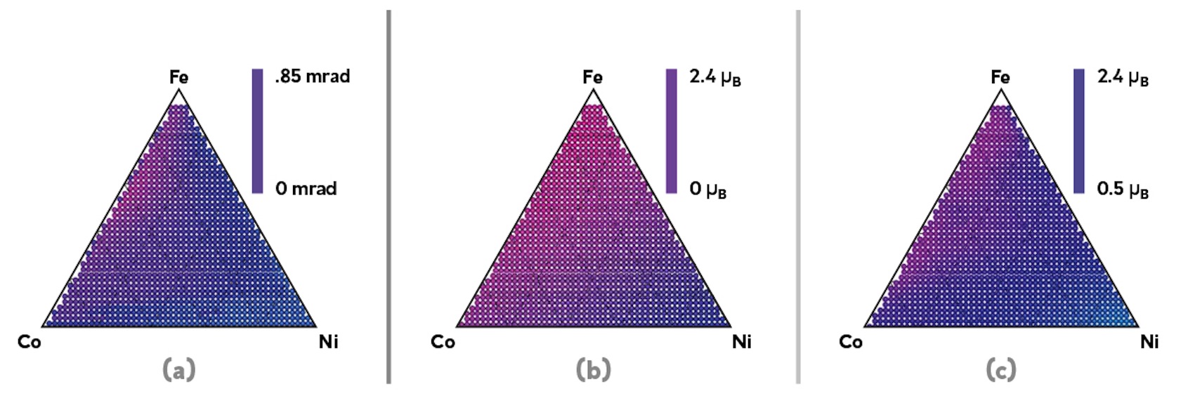
They tested their approach using a 100 nanometre-thin film made of iron, cobalt and nickel spread on a sapphire substrate. Various possible combinations of the three elements were distributed along the film. These ‘composition spread samples’ are used to test many similar materials in a single sample.
The team first conducted a simple high throughput technique on the sample called combinatorial X-ray diffraction. The resulting X-ray diffraction curves provide detailed information about the crystallographic structure, chemical composition, and physical properties of the sample.
The team then used machine learning to break down this data into individual X-ray diffraction curves for every combination of the three elements. High throughput calculations helped define the magnetic properties of each combination. Finally, calculations were performed to reduce the difference between the experimental and calculation data.
Their approach allowed them to successfully map the ‘Kerr rotation’ of the iron, cobalt, and nickel composition spread, representing the changes that happen to light as it is reflected from its magnetised surface. This property is important for a variety of applications in photonics and semiconductor devices.
The researchers say their approach could still be improved but that, as it stands, it enables mapping the magnetic moments of composition spreads without the need to resort to more difficult and expensive high throughput experiments.
Image caption: (a) Kerr rotation mapping of an iron, cobalt, nickel composite spread using the more accurate high throughput experimentation method, (b) only high throughput calculation, and (c) the Iwasaki et al. combined approach. The combined approach provides a much more accurate prediction of the composite spread’s Kerr rotation compared to high throughput calculation on its own.


