
Researchers make tiny light sources from HgTe quantum dots
Approach could be used to design new optical devices, detectors, and emitters based on IR-emitting QD-based microlasers
Scientists from Far Eastern Federal University (FEFU, Vladivostok, Russia), together with colleagues from FEB RAS, China, Hong Kong, and Australia, manufactured ultra-compact bright sources based on IR-emitting mercury telluride (HgTe) quantum dots, the future functional elements of quantum computers and advanced sensors. The work was published in Light: Science and Applications.
The near- and mid-IR spectral range has potential for making optical telecommunication devices, detectors, and emitters, as well as sensor and next-generation security systems. Semiconductor QDs represent promising nanomaterials emitting light exactly in this range. However, the main issue is associated with fundamental physical limitations (the Fermi golden rule, Auger recombination, etc.) dramatically decreasing intensity of the IR-emitting QDs.
The researchers have overcome this limitation by applying a special resonant lattice of nanostructures. Scientists formed the lattice by ultra-precise direct laser printing on the surface of a thin film of gold.
"The plasmon lattice we developed consists of millions of nanostructures arranged on the gold film surface. We produced such lattice using advanced direct laser processing. This fabrication technology is inexpensive comparing to existing commercial lithography-based methods, easily up-scalable, and allows facile fabrication of nanostructures over cm-scale areas. This opens up prospects for applying the developed approach to design new optical telecommunication devices, detectors, and emitters, including the first IR-emitting QD-based microlaser," said the author of the work, Aleksander Kuchmizhak, a researcher at the FEFU Center for Virtual and Augmented Reality.
The resonant lattice converts the pump radiation into a special type of electromagnetic waves referred to as surface plasmons. Such waves, propagating over the surface of the patterned gold film within the capping layer of QDs, provide their efficient excitation boosting photoluminescence yield.
"For the visible spectral range, quantum dots have been synthesising for several decades. Just a few scientific groups in the world, though, are capable of synthesising QDs for the near and mid-IR range. Thanks to the plasmon lattice we developed, which consists of plasmon nanostructures arranged in a special way, we are able to control the main light-emitting characteristics of such unique QDs, for example, by repeatedly increasing the intensity and photoluminescence lifetime, reducing the efficiency of non-radiative recombinations, as well as by tailoring and improving emission spectrum," said Alexander Sergeev, a senior researcher at IACP FEB RAS.
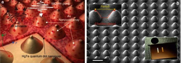
The picture above shows: a) an artist's impression of the HgTe QD layer coated above the laser-printed Au nanobump array; and b) Side-view (view angle of 45°) SEM image showing the Au nanobump array printed at a 1-μm pitch. A close-up SEM image on the top inset demonstrates the difference between the period and the 'effective' period of the nanobump array. The bottom inset shows a photograph of two large-scale nanobump arrays produced on the glass-supported Au film.


