
Novel photonics applications require vertical integration
Scalable assembly and packaging of photonic integrated circuits for emerging applications.
By Douwe Geuzebroek, Paul van Dijk, Arne Leinse at LioniX International B.V.
Photonic Integrated Circuit (PIC) technology is becoming more interesting for applications outside telecom and data communications. New applications for PICs in metrology and life science are emerging as the promise of technology scaling enables lower cost and smaller form factors that well match novel application roadmaps.
Growth beyond traditional PIC applications is possible due to maturing photonic IC technology and a greater number of foundries providing new Silicon Photonics, InP and Silicon-Nitride processes. Rather than surmounting technology hurdles, the challenge faced by PIC designers and manufacturers is how to best address the broad scope of novel applications now possible.
These emerging applications have a broad range of requirements both in terms of Photonic IC functionality and also in making interconnections with other parts of the system. There is no single interface in this broad scope of applications like those typical for standard fiber optic cables. Furthermore, these diverse requirements often mean that optimizing on-chip functionalities only will not be sufficient to address the complete need.
An integral or vertical approach needs to be applied to product designs that takes into account overall system performance and interface needs as well as the chip design itself. We show a different set of interfaces available in the TriPleX waveguide platform [1] that will match the requirements of emerging applications such as bio-photonics and confocal microscopy, flow cytometry, molecular diagnostics, bio-sensing, DNA sequencing and micro spectroscopy. We conclude with an example of the vertical integrated approach for broadband beamformers in 5G antenna and satellite communications systems.
Standard building blocks
PIC technology relies on the use of validated standard building blocks. These building blocks, such as waveguide bends, taper sections and modulators (amongst many) are designed with a common use in mind. However, in assembly and packaging of these PICs, the field of emerging applications is so broad that there is no standard packaging scheme that is suitable for all, unlike the fiber pigtailed butterfly package that is used across telecommunications.

Figure 1. Photograph of an assembled integrated OCT system. The inset photograph shows the PIC containing the arrayed waveguide grating structures used to spectrally convert the signal to the attached CCD array utilizing a hybrid approach.
Assembly interfaces for future applications
The most common interface to Photonic ICs is the optical fiber. Adding one or multiple fibers to a PIC is a very common method of interfacing with the device, especially in telecommunications applications, where fiber is the main light transport means. Many interconnection techniques have been used here such as the fiber array; others include using a v-groove array in glass or silicon to assemble fibers at a certain pitch or matching the waveguide pitch to the PIC.
However, these standard methods utilized in the infrared wavelength domain do not provide sufficient accuracy for interconnection requirements for visible light. Due to the application of lower wavelengths, the alignment tolerance decreases. Furthermore, the energy density increases due to the incremental photon energy at lower wavelengths; especially in the blue range within the color spectrum, any organic material like epoxies needs to be avoided. Through careful design of the interconnect region and polishing the PIC facets, assembly methods have been developed which avoid use of any epoxy in the light path.
A second interface type demonstrates a true advantage of using PICs when very small pitches between the waveguide outputs need to be applied. For instance, it is possible to create pitches 10 mm apart coming from a splitter device that has divided incoming light into multiple output beams. These multiple beams interfere in free space after leaving the PIC; a behavior of a multitude coherent point sources is observed.
At a certain distance, this creates interference which patterns the emitted light in relation to the amount of point sources and their relative phase. By changing the phase of each channel in the splitter, the interference pattern can be shaped, or moved – all without any mechanical moving parts.
The direct free-space interface can be taken one step further, introducing vertical out coupling of the light, using 45 degree micro-machined mirrors. In this way the light leaves the PIC perpendicular to the planar waveguide layer, from any location on the PIC. FIB (Focused Ion Beam) milling provides accurate control to define a smooth mirror at the correct angle, here at 45˚. Since the mirror functions based upon the principle of total internal reflection, no additional metal layers are needed, and an efficient mirror can be made.

Figure 2. Narrow linewidth tunable laser based on hybrid assembly of an InP gain section and a tunable mirror made in TriPleX.
Coupling light using a free space interface is also possible. For some high-end visible light applications, it is favorable to couple light into the PIC using lenses. For instance, one or several laser diodes can be accurately aligned via a lens system, focusing the light on the input facets of the PIC. A high-end lens system is an alternative to the use of simple ball lenses, which is a better choice when a compact and cost sensitive application is targeted.
Another approach for connecting the PIC to devices on top of the chip are grating couplers. For example: in low-cost, even disposable bio-photonic sensors, integrated optical devices allow for label-free, real-time measurement of multiple parameters simultaneously. For example, in evanescent field-based micro-ring resonator sensors, the parameter to be sensed influences the propagation properties of a guided light signal in the on-chip sensing region. NIR (850 nm) applications are very attractive for absorption measurements, as both high quality light sources (GaAs VCSELS) and detectors (silicon PIN photodiodes) are readily available at very attractive price levels. These VCSELs and detector arrays can be flip chipped onto the surface of the PIC using grating couplers to direct the light in and out of the waveguides. This flip chip mounting of the devices onto the substrate opens possibilities for mass production.Hybrid assembly
The flip chip placement of VCSEL sources and detector arrays is already a first step towards hybrid integration. This approach enables the design to integrate multiple PIC or other microsystems parts based on different technologies to generate a new product. In this way, each component does what it is doing best and the applications or product that is designed is using various technology building blocks to mix and match into a new targeted design. To demonstrate this further we will show three applications using this hybrid approach: Optical Coherence Tomography (OCT); a tunable, narrow linewidth laser; and a microwave photonic beamforming solution.
Optical coherence tomography
A promising application that can hugely benefit from photonic integration is OCT. This diagnostic method is the optical equivalent of the well-known acoustic echo (sonogram technology) that we use to picture our unborn children. In contrast to echoscope, OCT is a non-contact technology, making it applicable to eye research and retinal imaging as well, a ‘surrogate biomarker’ that could be used to detect Alzheimer’s and a complementary, and less-costly, method to produce PET scans of the brain as well as testing the cerebrospinal fluid taken from the base of the spine, which is currently used to detect deposits of beta amyloid protein, which can indicate Alzheimer’s. Since the OCT system relies on many optical components, it is well suited for integration.
The need for this is becoming evident when the size of the system needs to go down as the medical diagnostic tools need to transition out of hospital settings and towards point of care, such as a doctor’s office or neighborhood clinic. An OCT module has been realized based on hybrid assembly that attached a linear CCD array to the side of a PIC. In this example, a readout for the wavelength filter (based on an array waveguide grating) became possible. A broadband light source like a SLED was also attached using hybrid techniques to realize a complete OCT module the size of a mobile phone. See Figure 1 for an example of a prototype OCT system. The PIC holds the complete OCT system including arrayed waveguide gratings to separate the wavelengths from the broadband light source reflected by the target.
Narrow linewidth tunable laser
Another novel application resulting from a hybrid assembly approach is the narrow-linewidth tunable laser. This module combines an InP gain chip and a TriPleX tunable mirror into an external cavity laser, tunable over a wide range, with record-low linewidths as low as 40Hz [2]. This application requires interconnection of two chips of different material systems with low interconnect losses at the hybrid interface, which is inside the laser cavity. An example of the hybrid coupling is depicted in Figure 2, showing an InP gain section with one side coated to act as a mirror and the other side having an antireflection coating. The second mirror of the external cavity setup is constructed on the TriPleX chip and consists of micro-ring resonators and other structures to create a long cavity and a wavelength tunable mirror. The low-loss hybrid assembly, combined with the low-loss large cavity length, makes this laser a world record holder for narrow line width and tunability over a wide range [2].
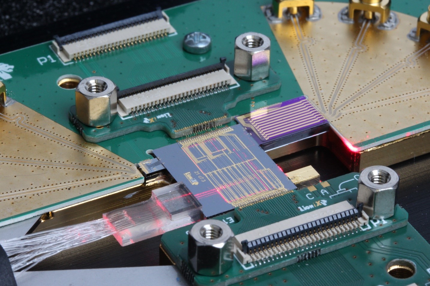
Microwave photonic beamformer
For next generation mobile networks and satellite communication systems, a broadband and continuously tunable beamforming element is required. The element needs to process several RF signals and align the appropriate signals to steer a beam coming out of a phased array antenna. The given requirements of current and upcoming systems make a good case to perform the processing within the optical domain where broadband and continuous phase changes can be realized using true time delays. An example approach is a cascaded microring resonator structure. As the required delays are long (in the order of several nanoseconds), a photonic integration platform is required that has low loss.

Figure 3. A RF-in/RF-out beamformer utilizing hybrid assembly to combine TriPleX true time delays and an InP laser, modulator and detectors.
In microwave beamforming, a fast modulator and detector for the signal conversion between RF and photonics is also required. The best solution is the hybrid assembly approach combining the low-loss TriPleX waveguide platform for true time delays and an InP platform to realize the active components: the modulator, detector and laser. Figure 3 shows an assembly of an RF-in/RF-out microwave photonic beamformer where the signal delays are processed in the optical domain. The full hybrid assembly principle based on co-operation of two PIC platforms as well as the driving electronics can only work when a vertical integrated design approach is taken. The latest results of the beamformer are given in the References section following this article’s conclusion; please see reference [3].
Conclusion
Applications that benefit from Photonic Integration technology are moving fast and opportunities are growing. Since the total scope of applications is also broadening outside of the tele- and data communications range, the different interfaces that connect the PIC to the other portions of the total system are also expanding outside of standard fiber interface approaches. Therefore, a vertically integrated design approach needs to be taken to combine the design, the manufacturing and the assembly of a PIC into a complete module to ensure that novel applications will benefit from the capabilities of photonic integration.


