Loading...
News Article

Plan Optik driving connectivity to the next level

News

Plan Optik AG, manufacturer of customized wafers from glass, quartz or glass-silicon compound materials launched its new Cu-Interposer technology at SEMICON Europa 2019.

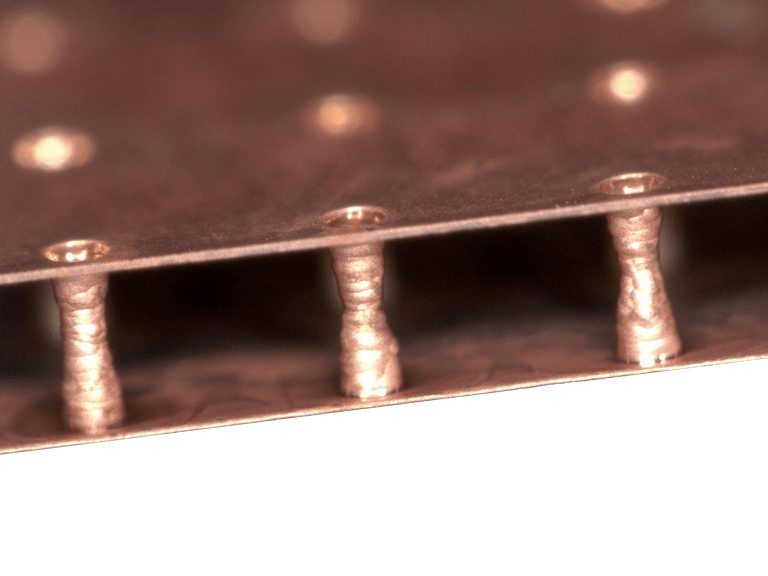
The progressive miniaturization, increasing integration density and requirements for more powerful signal routing create the need for 3D integration. Interposer technologies for rewiring have been developed for efficient communication with high transmission rates in the 3D chip stack or 3D system package. At present, organic interposers are predominantly used for these technologies. Organic interposers can be produced inexpensively, but are no match for the modern and increasing demands on 3D integration and high transfer rates. Through Glass Via Wafers (TGVs) offer a cost-effective alternative to the costly silicon interposer technology. TGV interposers are a promising technology for three-dimensional and high-density hybrid integration. For high-frequency applications and optoelectronic components, insulation layers are integrated and therefore not required compared to silicon technology of IC chips.

But: There is no established solution to produce glass interposers at wafer level, which provides all the required properties for high-frequency applications. For this reason, Plan Optik has developed a new technology to produce interposers with an applied copper layer, which is particularly suitable for high-frequency applications.

Next Generation Interposer

As a first step, Plan Optik will be able to offer Interposers as drilled glass wafers with a copper layer. Those Interposer wafers will be available in sizes up to 300 mm with hole diameters down to 100 µm (depending on wafer thickness). At present, customized Redistribution Layers (RDL) can be integrated on wafer sizes up to 8”. The wafer thickness ranges from 200 µm up to 1 mm. Plan Optik’s Cu-Interposer can be produced as a wafer, as panels or as boards depending on customer needs. With a minimum hole distance equal to via diameter and a Cu-layer thickness starting from 1 µm Cu-Interposer are perfectly suitable for high-frequency applications like for example 5G broadband transmission, radar and imaging sensors, biosensors or beam steering networks.

Quintessent appoints Bob Nunn chief operating officer
PI to demonstrate new PIC alignment system at Photonics West
Drut launches 2500 product series with CPO for AI datacentres
III-V Epi advocates GaAs for new lasers
Marvell announces new CPO architecture for custom AI accelerators
Printing high-speed modulators on SOI
Photon IP raises €4.75m for advanced PICs
ANELLO Photonics launches Maritime Inertial Navigation System
Aeluma joins AIM Photonics as full industry member
Imec makes breakthrough with GaAs lasers on silicon
POET acquires Super Photonics Xiamen
Voyant Photonics launches affordable Carbon LiDAR
Penn State makes breakthrough in photonic switching
New nanocrystals could lead to more efficient optical computing
QCi awarded NASA contract to apply Dirac-3 photonic optimisation solver
The Netherlands launches ChipNL Competence Centre
TOPTICA to create chip-integrated lasers for quantum PIC project
NSF selects six pilot projects for National Quantum Virtual Laboratory
SiLC Technologies launches Eyeonic Trace Laser Line Scanner
Southwest Advanced Prototyping Hub awarded $21.3 million CHIPS Act funding
Cambridge Graphene Centre and CORNERSTONE to participate in PIXEurope
Cost-effective lasers for extended SWIR applications
IBM unveils co-packaged optics technology for AI and datacentres
QCi announces $50 million concurrent stock offerings
CHIPS Act funding to be awarded to Coherent, Skywater, and X-Fab
ERC consolidator grant awarded for optoacoustic neural network project
Imec demonstrates InP chiplet integration on 300 mm RF silicon interposer
Ayar Labs raises $155 million for optical I/O
Celestial AI awarded 2024 Start-up to Watch by Global Semiconductor Alliance
Researchers develop “last missing piece” of silicon photonics
Quantum sensors for controlling prosthetics
UPVfab to participate in European Commission photonic chips project

×
Search the news archive

To close this popup you can press escape or click the close icon.
Logo
x
Logo
×
Register - Step 1

You may choose to subscribe to the PIC Magazine, the PIC Newsletter, or both. You may also request additional information if required, before submitting your application.


Please subscribe me to:


You chose the industry type of "Other"

Please enter the industry that you work in: