
'Tsunami' on a silicon chip: a world first for light waves
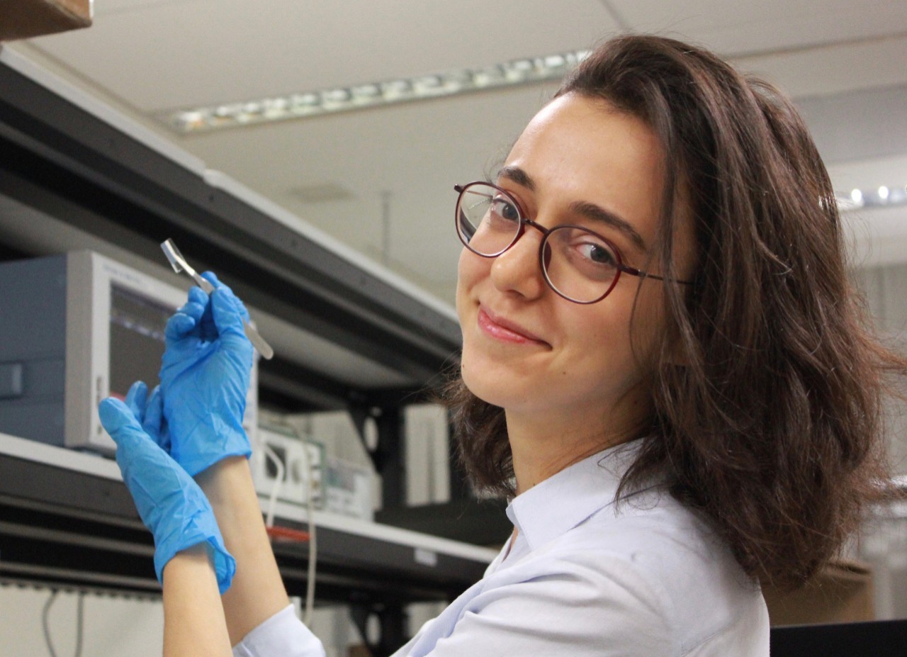
Ezgi Sahin, a PhD student at Singapore University of Technology and Design.
A collaboration between the Sydney Nano Institute and Singapore University of Technology and Design has for the first time manipulated a light wave, or photonic information, on a silicon chip that retains its overall 'shape'.
A tsunami holds its wave shape over very long distances across the ocean, retaining its power and ‘information’ far from its source.
In communications science, retaining information in an optic fibre that spans continents is vital. Ideally, this requires the manipulation of light in silicon chips at the source and reception end of the fibre without altering the wave shape of the photonic packet of information. Doing so has eluded scientists until now.
A collaboration between the University of Sydney Nano Institute and Singapore University of Technology and Design has for the first time manipulated a light wave, or photonic information, on a silicon chip that retains its overall ‘shape’.
Such waves – whether a tsunami or a photonic packet of information – are known as ‘solitons’. The Sydney-Singapore team has for the first time observed ‘soliton’ dynamics on an ultra-silicon-rich nitride (USRN) device fabricated in Singapore using state-of-the-art optical characterisation tools at Sydney Nano.
This foundational work, published in Laser & Photonics Reviews, is important because most communications infrastructure still relies on silicon-based devices for propagation and reception of information. Manipulating solitons on-chip could potentially allow for the speed up of photonic communications devices and infrastructure.
“The observation of complex soliton dynamics paves the way to a wide range of applications, beyond pulse compression, for on-chip optical signal processing,” Ms Sahin said. “I’m happy to be a part of this great partnership between the two institutions with deep collaboration across theory, device fabrication and measurement.”

Professor Ben Eggleton and Professor Dawn Tan.
Co-author of the study and Director of Sydney Nano, Professor Ben Eggleton, said: “This represents a major breakthrough for the field of soliton physics and is of fundamental technological importance.
“Solitons of this nature – so-called Bragg solitons – were first observed about 20 years ago in optical fibres but have not been reported on a chip because the standard silicon material upon which chips are based constrains the propagation. This demonstration, which is based on a slightly modified version of silicon that avoids these constraints, opens the field for an entirely new paradigm for manipulating light on a chip.”
Professor Dawn Tan, a co-author of the paper at SUTD, said: “We were able to convincingly demonstrate Bragg soliton formation and fission because of the unique Bragg grating design and the ultra-silicon-rich nitride material platform (USRN) we used. This platform prevents loss of information which has compromised previous demonstrations.”

Artist's impression of the Bragg gate on a silicon substrate.
Solitons are pulses that propagate without changing shape and can survive collisions and interactions. They were first observed in a Scottish canal 150 years ago and are familiar in the context of tsunami waves, which propagate thousands of kilometers without changing shape.
Optical soliton waves have been studied since the 1980s in optical fibres and offer enormous promise for optical communication systems because they allow data to be sent over long distances without distortion. Bragg solitons, which derive their properties from Bragg gratings (periodic structures etched in to the silicon substrate), can be studied at the scale of chip technology where they can be harnessed for advanced signal processing.
They are called Bragg solitons after Australian-born Lawrence Bragg and his father William Henry Bragg, who first discussed the concept of Bragg reflection in 1913 and went on to win the Nobel Prize in Physics. They are the only father and son pair to have won Nobel Prizes.
Bragg solitons were first observed in 1996 in Bragg gratings in optical fibres. This was demonstrated by Professor Eggleton while he was working on his PhD at Bell Labs.
The silicon-based nature of the Bragg grating device also ensures compatibility with complementary metal oxide semiconductor (CMOS) processing. The ability to reliably initiate soliton compression and fission allows ultrafast phenomena to be generated with longer pulses than previously required. The chip-scale miniaturisation also advances the speed of optical signal processes in applications necessitating compactness.
Funding declaration
Ezgi Sahin acknowledges scholarship funding Singapore International Graduate Award (SINGA) from A*STAR and thanks the Institute for Photonics and Optical Science (IPOS), the University of Sydney Nano Institute and the School of Physics at the University of Sydney for hosting her to conduct the experiments with Andrea Blanco Redondo. Dawn Tan acknowledges the support of the National Research Foundation Competitive Research Grant, MOE ACRF Tier 2 grant, SUTD – MIT International Design center, Digital Manufacturing and DesignGrant and the National Research Foundation, Prime Minister’s Office, Singapore, under its Medium Sized Centre Program. Ben Eggleton acknowledges the support of the Australian Research Council (ARC) Laureate Fellowship (FL12010)


