
Fraunhofer HHI technology in an all-optical RAM cell
Developments in the computer industry have allowed processor power to grow exponentially for years. This development raises the fundamental issue of the “memory wall”. The memory wall imposes a built-in bottleneck. As a consequence, aspects of CPU-memory interchange such as data buffering and lookup operations run significantly slower. In an era of big data and high-bandwidth communications, this problem will only become more urgent.
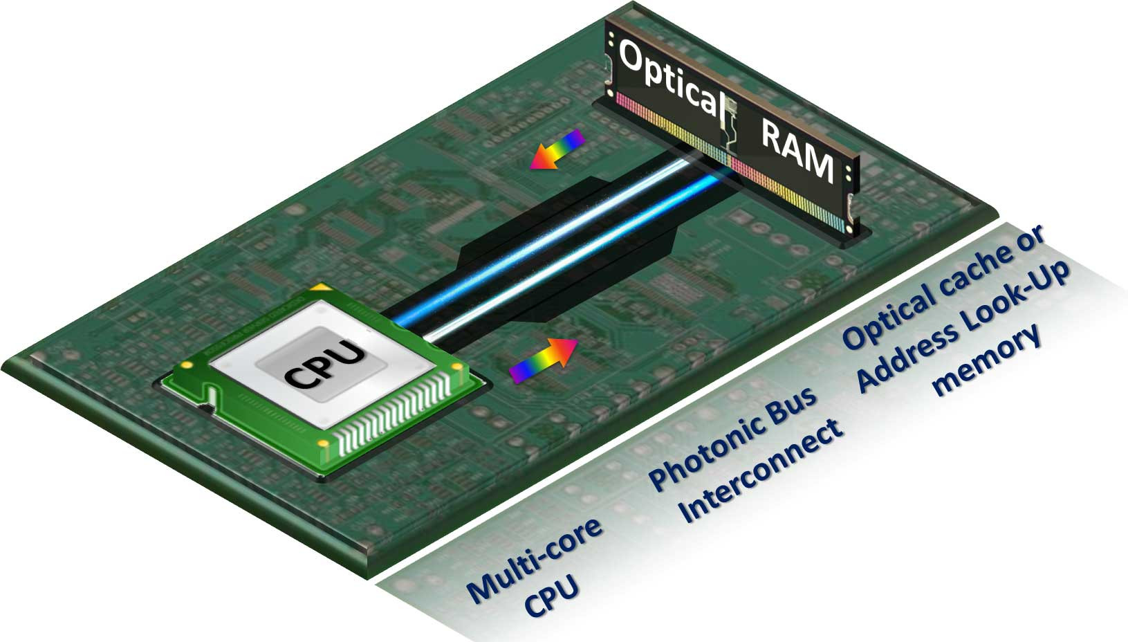
A research team from the Aristotle University of Thessaloniki, Greece, is working on a solution using Fraunhofer HHI technology. It developed an architecture, based on optics, which allows breaking through the memory wall. Recently, the team presented an all-optical RAM cell architecture that was able to double the speed of electronic RAMs. What makes this approach so effective is that the team employed the optical wavelength dimension. In the device the inverse signals are generated at two different wavelengths for bit and for bit-bar and sent through a single channel, with random access controlled through a fast optical push-pull gate.
The proof-of-concept device, which is using chip designed with the help of Fraunhofer HHI foundry services, is composed of a single optical RAM cell. This cell includes a semiconductor optical amplifier Mach-Zehnder interferometer (SOA-MZI) that functions as an access gate. This gate is connected, via an arrayed waveguide grating (AWG), to an indium-phosphide set-reset optical flip-flop unit. It was able to demonstrate all core four RAM operations: reading, writing and random-access. It was doing this at twice the rate of comparable devices - rates of some 10 Gbit/s.
Currently however, this proof-of-concept device has a larger footprint and higher per-bit energy consumption than electronic alternatives. The researchers want to address this flaw with the help of photonic-integration. One solution could be to keep the memory in the all-optical domain, which would thus eliminate the need for such conversion going into and out of the memory. This could be achieved by replacing the semiconductor optical amplifiers on the chip with integrated-photonic technologies and materials such as photonic crystals and phase-change memories.
Application areas include high-performance computers, and high-end routers as well as speeding up pseudo-random binary sequence (PRBS) generators for testing and encryption.
Fraunhofer HHI appreciates funding from the BMBF “Forschungsfabrik Mikroelektronik”.


