VCSEL inspection

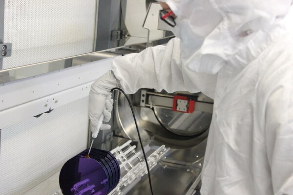
France-based company Unity-SC, which specializes in optical inspection tools for semiconductor wafer production, says that its new system will be able to increase yields in laser diode manufacturing.
The Grenoble firm says that its “LIGHTsEE” equipment, which is based on phase shift deflectometry (PSD), can spot otherwise “invisible” defects in vertical cavity surface-emitting laser (VCSEL) wafers.
Device demand
While they have been used in short-range optical communications for many years, demand for VCSELs is expected to increase dramatically as the devices find use in smart phone facial security systems, and possibly in lidar units for self-driving cars in the future.
In recent years manufacturers including Lumentum, Finisar, II-VI, and Trumpf subsidiary Philips Photonics have all announced plans to invest heavily in VCSEL production to meet that anticipated demand. The UK-based specialist wafer foundry IQE also has plans to quickly ramp VCSEL epiwafer production for its various clients as demand mushrooms.
Now Unity-SC says that its tool - tested by an unspecified device manufacturer - will help increase production yields, ultimately improving reliability and reducing the cost of the lasers and the systems that are built around them.
The emerging market for VCSELs inside lidar units for autonomous vehicles is said to be growing fast, but will also place a particular emphasis on failure-free operation, for obvious safety reasons.
Unity-SC says that topographical defects, which do not absorb or scatter light, are simply not visible when VCSEL wafers based on gallium arsenide material are probed with conventional optical inspection tools.
“While they have little impact on the structural quality of the substrate itself, they can lead to device failure later on [in] the process,” claims the firm. “For example, during the production of the Bragg grating reflectors, these topographic defects can lead to [an incorrect] Bragg period or, in some specific cases, to stress-induced cracks. These failures can happen during the process or after system delivery under heat or stress conditions, resulting in system failure.”
Fringe pattern
But thanks to the PSD technique, such defects can be easily detected, Unity-SC claims. “The PSD provides a full wafer, non-contact, high-throughput solution with a height sensitivity below 5 nm,” adds the firm. “Since the acquisition is made without moving the substrate, it is stress-free and compliant with any fragile substrate.”
PSD works by projecting a fringe pattern onto a target surface, and then capturing the reflected patterns. Shifting the phase of the illuminating pattern and then retrieving the phase distribution in the reflected pattern yields topographical details of the target surface - for example sudden changes in slope that could result in a defect later on in the wafer fabrication process.
Unity-SC claims that in the tests carried out with a major VCSEL producer, its PSD technology delivered improved yields and a decrease in device failures.


