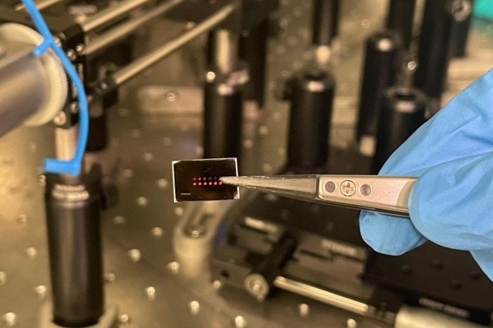
Plasmonic technology opens the way to mass manufacture of high-performance chips

EU-funded researchers have created a ground breaking platform to meet industry’s need for low-energy, small-size, complex and high-performance circuits.
Photonics technology plays an important role in the European and global economies, driving innovation in sectors such as ICT, medicine, energy, military, manufacturing, agriculture and space. As its use spreads, it becomes increasingly important to find ways to mass produce photonics devices at low cost. This implies merging the technology with standardised production processes that are compatible with advanced electronics integrated circuit technologies. In other words, combining photonic and electronic functionalities in one chip.
The problem lies in incompatible dimensions. While electronic chip sizes are measured in nanometres, photonics chips exist in the order of micro- or millimetres. The EU-funded PLASMOfab project took up – and overcame – this challenge with the help of plasmonic technology. Ten industrial partners and academic and research institutes combined their know-how and expertise in photonic integrated circuits (PICs) and optoelectronics to create a plasmo-photonic chip. Now successfully completed, the project has made the mass manufacture of these high-performance components possible.
The PLASMOfab team’s work has brought about great advances in the technology used in optical data communications and biosensing for point-of-care applications. It has developed plasmonics that are compatible with complementary metal-oxide-semiconductor (CMOS) technology already used in electronics, and has used this technology to consolidate advanced PICs with electronic ICs in mass production. Standardised CMOS processes were used to merge CMOS-compatible metals like aluminium, titanium nitride and copper, and photonic structures with electronics.
A major achievement of the project was the development of a novel ultra-compact plasmonic transmitter. The device has a footprint of 90 x 5.5 µm² and transmits 0.8 TBit/s (800 Gbit/s) through 4 individual 0.2 TBit/s transmitters. The project team also demonstrated how low propagation losses can be achieved using CMOS-compatible aluminium plasmonic waveguides co-integrated with silicon nitride photonics. Their findings were published in the journal ‘Scientific Reports’.
“PLASMOfab’s main goal has been to address the ever increasing needs for low energy, small size, high complexity and high performance mass manufactured PICs,” said Assistant Professor Nikos Pleros of project coordinator Aristotle University of Thessaloniki, Greece, in a press release posted on the ‘Synopsys’ website. “We have achieved this by developing a revolutionary yet CMOS-compatible fabrication platform for seamless co-integration of active plasmonics with photonic and electronic components.”
The partners expect that by further developing this technology they will be able to demonstrate the marked advantages that CMOS-compatible plasmonics have when applied to PICs. “When the best of all three worlds of plasmonics, photonics, and electronics converge in a single integration platform, PICs with unprecedented performance and functionality will be realized, targeting a diverse set of applications and industrial needs while meeting mass production requirements,” explained lead researcher Dr Dimitris Tsiokos of Aristotle University.
PLASMOfab (A generic CMOS-compatible platform for co-integrated plasmonics/photonics/electronics PICs towards volume manufacturing of low energy, small size and high performance photonic devices) concluded in December 2018. Its research has led to the launch of two new companies whose goals will be to commercialise the new technologies.


