
A New Raman Spectroscopy Approach Shrinks the System Onto a Chip

A newly-patented imec concept utilizes silicon photonics and thousands of tiny interferometers to reduce a Raman spectroscope to the size of a smartphone.
By: Els Parton, Harrie Tilmans & Pol Van Dorpe


Raman Spectroscopy is a time-tested means to analyze the composition of materials using a portion of light reflected from a sample into the instrument. Today’s most commonly available, highly accurate Raman spectroscopes are desktop-sized and expensive; handheld versions suffer from performance limitations and are also costly. Unlike existing handheld spectroscopes, imec’s new concept exhibits the high optical throughput and spectral resolution of a desktop system, opening a whole new range of applications in which complex samples can be analyzed with a more affordable handheld device.
From medieval paintings to drugs
Raman spectroscopy was discovered by C. V. Raman in 1928, which earned him the Nobel Prize for Physics in 1930. Raman spectroscopy is used to identify materials – fluids, powders, solids – and to learn more about the materials composition. Today’s spectroscopes shine laser light on the material, and by analyzing a specific part of the scattered light, a spectral chart can be made. The scattered light that is analyzed is the so-called ‘Raman scatter,’ which is characterized by a different wavelength than the laser’s wavelength. It originates from the molecular vibrations in the material. One can recognize the spectral ‘fingerprint’ of each material and compound in the spectral chart.
Raman spectroscopy is used in many different fields – in fact, it can be used in any application where non-destructive material analysis is needed. For example: in pharmaceutics, Raman discloses the distribution of active compounds in medicinal tablets. Raman can also classify meteorites in chondrites and achondrites based on its mineral composition. It can even dive into the kind of hybridization in a (carbon) molecule and tell whether it’s a sp2 or sp3 hybridization. In semiconductor R&D, Raman spectroscopy can be used to determine the electrical properties and the number of layers of graphene, or characterize the stress in specific layers. In life sciences, Raman is able to tell something about the interaction between cells and specific drugs. In art work, the technique is used to identify which pigments were used, which in turn can give an indication about the artist’s identity, his working method, and the age of the work. Even the mummified skin of ‘Otzi the Alpine Iceman’ was examined with Raman spectroscopy.
Existing devices: desktop and handheld
Numerous Raman spectroscopes are available today, specifically tuned to varied applications. Raman systems are often implemented as a microscope where the sample is illuminated with a diffraction limited spot and the Raman photons are collected with a high NA (numerical aperture) objective. Next to these desktop devices (which make up the largest part of the market), handheld counterparts have also emerged. These are really convenient for research ‘in the field’ like in the case of art work studies or archeology.
As is often the case with miniaturized versions of measuring equipment, handheld Raman spectroscopes are not as good as the desktop versions. For the study of the pigments in paintings, they work fine because the pigments generate strong Raman signals, but for more complex samples such as opaque fluids (such as milk), skin or powders, the current systems are not adequate or need a long measuring time. Also, the high pricing of handheld Raman spectroscopes inhibits widespread use.
What if a cheap but high performance handheld Raman spectroscope was available? Which new applications would be made possible? Think of food screening ‘on the go,’ skin screening for melanoma at the general practitioner’s office, or screening for drug authenticity by authorities throughout the supply chain. Within the food and beverage industry, it can be used for characterization purposes and for identifying and evaluating the authenticity, safety and quality attributes for a broad range of food and agricultural products. For instance, Raman is an ideal technique to identify and indicate the adulteration of edible oils or to determine the level of alcohol in beverages. Multiple component analysis using Raman spectroscopy is key (for example) in understanding the quality of milk by determining the fat, protein and water content of the milk a cow or a goat is producing (in real time). For cosmetics, Raman spectroscopy can be used for verification of the purity of ingredients such as those used in personalized moisturizing creams and essential oils (eucalyptus, ginger, lavender, basil, vanilla). Furthermore, it can be used to determine the remaining concentration of solvents in pharmaceutical preparations to decide if the level of nutrition is sufficient for a certain cell culture to maintain their growth.
Why is it difficult to further improve current handheld devices?
There are two main challenges in developing Raman systems. First of all, spontaneous Raman scattering is typically very weak, and as a result the main difficulty of Raman spectroscopy is separating the weak inelastically scattered light from the intense Rayleigh scattered laser light.
Secondly, in strongly scattering media, such as food or human tissue, the incident photons are not confined in a small spot, but instead generate a blurred spot, with sizes up to several millimeters. This increases the “optical throughput” or “etendue,” which is a measure for the spread of the light in space and angle. A spectrometer usually limits the etendue, which drops for compact devices.
In commonly used dispersive spectrometers, the light is focused on a slit, and its spectral components are separated using a diffraction grating. Miniaturization of a high spectral resolution device (<1 nm) requires a reduction in the slit width, thus reducing the etendue.
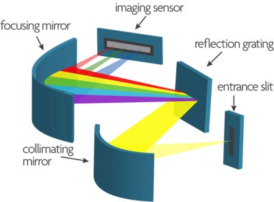
Figure 1: Existing dispersive handheld spectrometers make use of entrance slits, mirrors, and gratings like those indicated in this scheme. In this way, the etendue and spectral resolution are coupled through the size of the entrance slit. Downscaling of the spectrometer leads to lower spectral resolution or acceptance etendue.
Ultimate miniaturization of optical devices can be realized using integrated photonics and waveguides. The etendue of a single-mode waveguide (which is the ultimate scaling of this approach) equals approximately λ², with λ the wavelength. If the used wavelengths is (for example) 860nm, this results in an etendue of 7.3e-7 mm²sr, which is 106-107 times lower than required for analyzing diffuse scattering samples.
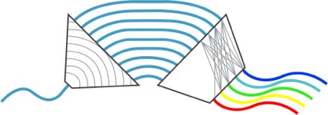
Figure 2: Existing photonic-based handheld spectrometers are limited in miniaturization by the etendue of single-mode waveguides.
A spatially heterodyne spectrometer based on silicon photonics
Because of the limitations of current approaches in handheld Raman spectrometers, other concepts have been investigated. Another class of spectroscopy is based on light interference and implemented (for instance) in Fourier transform spectroscopy or in spatially heterodyne spectroscopy. These concepts exhibit an intrinsically larger etendue and are therefore more ‘scaling proof’.
A well-known Fourier Transform spectrometer is based on the Michelson interferometer. A beam of light is divided into two beams that take different paths before coming together and interfering. This enables tiny differences in the wavelength to be measured. The disadvantage of this design – particularly if you want to miniaturize it – is that two mirrors are used, one of which moves.
Researchers from imec have now developed an integrated photonics version of such a scheme without moving parts: the integrated spatially heterodyne spectrometer. The etendue is less limited in this case and equals n x λ², with n being the number of interferometers. As mentioned above, if the used wavelength is (for example) 860nm, and the preferred etendue (for complex samples) is around 0.5 mm²sr, then about a million interferometers would be needed.
This massive parallelization is possible with integrated photonics. The patented solution monolithically integrates close to a million interferometers on top of CMOS image sensors and light is delivered using micromirrors.
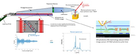
Figure 3: Concept of the patented solution made by imec researchers for a handheld Raman spectrometer, using a million interferometers on top of a CMOS image sensor. This build-up allows for extreme miniaturization without compromising on the etendue of the sample. This way, complex samples can also be measured. Furthermore, by using chip technology, the price of the device can be much lower than current devices.
This is the working principle of the newly developed Raman spectrometer: Laser light (785nm wavelength) is focused on a sample and the scattered photons are collected and collimated by means of a compound parabolic concentrator (CPC). After filtering the Rayleigh photons (at 785nm), Raman photons are directed to the on-chip waveguide (WG) access ports using a wedge-shaped light guide and chip-integrated micromirrors. By a proper choice of the wedge shape and the angle of the incident light, the micromirrors are able to redirect the light with a large efficiency (>50%), where it is coupled into the WGs thru gratings linked to individual single mode WG interferometers. The interferometers exhibit a range of lengths, allowing for reconstruction of the original spectrum. Their outputs are aligned with the pixel pitch of the integrated CMOS image sensor serving as a highly parallelized detector array. The chip is wire-bonded to a PCB and connected to a custom designed read-out board to capture the data and transfer it to a computing device, which reconstructs the spectrum and displays the required property.
Silicon nitride is the material of choice for the waveguides
Due to requirements of CMOS compatibility and visible transparency, silicon nitride was chosen as the waveguide material. The WG stack is built monolithically on top of the BEOL of 200mm front side illuminated CMOS image sensor wafers. Post-processing is done in a 200mm CMOS pilot line, using 193nm DUV lithography for patterning the WGs and grating couplers.
The spectrometer chip is constructed using SiN-based waveguide photonics, implemented on top of a CMOS image sensor (CIS) used for electrical readout. The spectrometer chip as used in the current design consists of an array of massively parallel evanescently-coupled Fabry-Perot interferometers, varying in length in the range 2.2-152.8µm (in linear steps of 0.2µm). Incident light is coupled into the waveguide structures using a grating based in-coupler (GC). Sloped metal output mirrors are used to couple the light from the waveguide to the readout pixels of the CIS (see also insert with a cross-section of the chip in figure above). An illustration of the layout showing a top view of the F-P resonators together with the grating in-coupler and sloped metal output mirror is shown in the figure below.
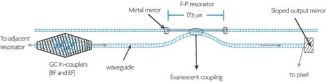
Figure 4: Part of the spectrometer chip layout, showing an evanescently coupled Fabry-Perot resonator (17.6µm long) together with the grating in-coupler(s) and the sloped output mirror for coupling the light to the pixels.
Conclusions
Raman spectroscopy is a powerful analytical technique with numerous applications. Existing desktop devices are rather bulky and have a price range of a few hundred thousand dollars/euros. The handheld solutions that exist today fail to reach the desired performance for high-end applications. Thanks to a new concept, it is now possible to overcome this performance barrier. By massive parallelization of waveguide interferometers integrated monolithically on top of a CMOS image sensor, both high optical throughput and high spectral resolution can be reached in a miniaturized device. This novel system is built in imec’s SiN biophotonics platform that guarantees robustness and compatibility with high-volume manufacturing.
Acknowledgements
Part of the work was performed under the EU-funded IoSense project; the authors acknowledge the funding received from the Electronic Component Systems for European Leadership Joint Undertaking (ECSEL-JU) under grant agreement No 692480 (Project Acronym: IoSense). This Joint Undertaking receives support from the European Union’s Horizon 2020 research and innovation programme as well as Germany, The Netherlands, Spain, Austria, Belgium, and Slovakia.
About Els Parton
Els Parton received her engineering degree and PhD at the KU Leuven, Belgium. She joined imec in 2001 as a scientific editor. In addition to writing numerous articles on imec research, she is editor-in-chief of imec magazine, a digital magazine published every month. www.imecmagazine.com
About Harrie Tilmans
Harrie Tilmans received his Ph.D. degree in Electrical Engineering from the University of Twente, The Netherlands. He has held R&D positions at the University of Twente, Boston University, the University of Wisconsin-Madison, Johnson Controls Inc (Milwaukee), the Catholic University of Leuven (Belgium), and CP Clare Inc (Hasselt, Belgium). His research covered MEMS resonators and resonating sensors, micro relays and RF-MEMS switches; MEMS and ultrasound transducer modeling and simulation, MEMS-CMOS process integration technology, MEMS packaging and assembly technology as well as integrated photonics. He has been with imec (Leuven, Belgium) since September 1999, first as Team Leader, then as imec Principal Scientist and Program Manager. He has managed and still manages several MEMS and photonics system based (industrial and funded) projects, more recently in the life sciences field. He has co-authored over 250 papers and issued over 20 patents. In 2001 he received the Eurosensors XV Fellow award for his pioneering work on microresonators.
About Pol Van Dorpe
Pol Van Dorpe received his PhD at the faculty of engineering of KU Leuven for his work in the field of spintronics. Afterwards he was appointed as a postdoctoral fellow of the FWO-Flanders (2006-2012), based in imec, and focused on metal based nanophotonics, or plasmonics for biosensors and energy harvesting. During this period he worked for some time at Stanford University and he established world-wide collaborations with renowned scientists in this field.
His work has led to over 140 peer-reviewed papers in high impact factor journals and has attracted more than 5000 citations. Since 2012 he has held a position as part-time associate professor at the physics department of KU Leuven; he is active as a principal member of staff in the life sciences department of imec where he leads a team working on experimental biophotonics. His main research focus is enabling novel applications in the life sciences field using integrated photonic concepts.


