
The zettabyte is not enough
The Fraunhofer Heinrich Hertz Institut (HHI) is at the forefront of optochip and photonic integrated circuit (PIC) research. Executive Director Martin Schell provides insight into the Institut's latest work with EMLs, EAMs and Mach-Zender modulators between 25 and 100 GBit/sec.
'Annual global IP traffic will reach 3.3 Zbyte per year by 2021' This forecast recently published by Cisco [1] looks like a huge market for transmitters, and receivers alike. On a closer inspection, however, optical component makers may get less excited. Thanks (or owing) to fantastic achievements on the high-speed performance of key components in recent years, single transmitter devices of fairly manageable design are capable today of delivering a modulation rate on the order of 50 Gb/s -100 Gb/s, and even beyond that when using more complex configurations.
Much of the IP traffic ends in data centers. Their typical architecture requires top-layer intra-center optical connections of 500 m to 2 km distance, and of up to 40-80 km between such facilities. Single-mode operation is of course compelling here. A simple calculation reveals that supporting a yearly data volume of 3.3 Zbyte, equivalent to an average data rate of about 8.3x1014 bit/s, would "“ theoretically "“ only need some 16,000 pieces of 50 Gb/s transmitter chips. With electro-absorption modulated lasers (EML), outlined below, these could be accommodated on a single wafer of 3-inch diameter, today's standard size in InP technology.
In the end, the situation will not be as bad like that: One north-south bit may cause hundreds of east-west bits; the same bit may pass a couple of transmitters; and data centers should be equipped to handle peak traffic. A recent analysis of AIM Photonics Academy [2] concludes that for the data centers operated by the four giants: Amazon, Facebook, Google, and Microsoft, there will be a demand of approximately 22m pieces of 100 Gb/s transceivers per annum, translating into a lower 4-digit 3" wafer quantity. With 8 wafers grown in a single run, this would correspond to about 150 of 4-hour epitaxy runs per year for the base wafer.
Silicon Photonics (SiP) is being widely regarded as the technology of choice for implementing intra-datacenter transceivers using electro-optic modulators for data generation. Despite tremendous progress made during the past years, SiP is lacking the ability to make practical Si-based lasers, and in fact there is no solution in sight. Consequently, InP-based source lasers have to be incorporated, either by demanding hybrid assembly techniques or by a hetero-integration (e.g. wafer bonding) approach. While the former represents a serial manufacturing process the latter requires additional on-wafer InP processing which questions the economic advantages of the Si core technology. InP technology, on the other hand, provides the only material platform enabling true monolithic laser integration. This enables extremely efficient and small-footprint ultrahigh-bitrate transmitter chips. Whereas directly modulated DFB laser devices may be useful up to 25 Gb/s, EML structures are predestined for achieving much higher modulation rates and concomitantly higher transmission distances, thanks to the adjustability of zero and even negative modulation chirp.
Fraunhofer HHI has been pursuing an intense program to develop EMLs over almost a decade. A fairly simple design has been adopted that uses an identical layer structure for both the DFB source laser and the electro-absorption modulator (EAM). The active region consists of InGaAlAs quantum well layers. With etching an isolation trench between the DFB and the EAM section as a key manufacturing step on top of standard lasers, EMLs now have developed into reliable high-yield devices [3].
Typical performance parameters of HHI's EML devices, featuring a 300 µm long DFB laser and an 80"¦120 µm long EAM section, are characterized by a static extinction ratio of > 20 dB at an EAM voltage swing of 2 V. A typical bias voltage is about -1 V, and below this point the chirp factor tends to become zero, and even negative when further shifting the bias towards larger negative values. The optical output power reaches some 5 dBm, generally limited by the fact that the DFB laser is not operated at optimum gain but is detuned to longer wavelengths to guarantee transparency of the electro-absorption modulator in the on-state.
To overcome that design-inherent issue, an optical booster amplifier has been added (Fig. 1) which provides output powers of >10 dBm. Even at 56 Gb/s the integrated amplifier does not affect the modulation behavior [4].
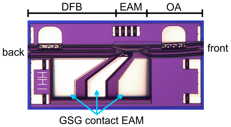
Figure 1: Top view of HHI's EML chip comprising an optical amplifier (OA) section to boost the output power. All of the three sections (DFB, EAM, OA) are made of the same layer structure, with electrical separation between them achieved by isolation trenches. The optical output is tilted to help suppress optical back-reflection. RF feeding of the EAM part is supported by a Ground-Signal-Ground (GSG) transmission line.
Thanks to this upgrade, next-generation PON requirements (average modulated output power of min 9 dBm @10 Gb/s; 1577 nm) can readily be met. The modulation rate of 56 GBd is routinely achievable now. However, a baud rate of 100 GBd has been demonstrated very recently (Fig. 2) after introducing further design refinements.
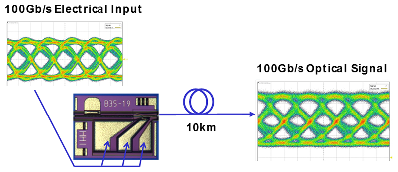
Figure 2: Demonstration of 100 Gb/s EML modulation capability (NRZ; λ=1300 nm; chip size: 420 µm x 320 µm)
Hence, a single-wavelength 100 G transmitter (on-off keying) may be implemented using a single tiny EML chip, provided suitable electrical drivers are available. In addition or instead, however, virtually all the common multiplex methods are applicable to efficiently accomplish even higher data rates and/or to exploit lower baud rates. 4- and 8-level Pulsed Amplitude Modulation (PAM) was successfully demonstrated on HHI's EMLs. Using a proprietary SiGe based driver IC, clear 32 GBd PAM4 eye diagrams have been achieved at a driver power of 84 mW leading to a figure-of-merit of 1.3 pJ/bit (Fig. 3).
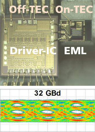
Figure 3: EML chip with co-packaged PAM4 driver IC designed at HHI. Power consumption of the driver IC is 84 mW (top); PAM4 eye diagram received at 32 GBd (bottom)
For space-division-multiplexed transmission, a serial dual-EML chip has been designed that comprises two EAMs in back-to-back configuration sharing the same DFB source laser between them [5]. Simultaneous modulation without mutual interference was demonstrated at 56 GBd (Fig. 4).
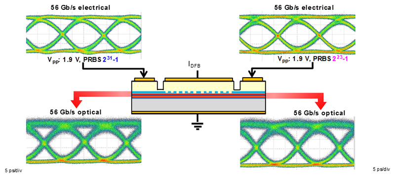
Figure 4: Dual-EML device sharing a common DFB source laser
For PAM4 schemes, a parallel 4-EML array was fabricated [6] which is capable of delivering an aggregated data rate of 224 Gb/s (4x 56 GBd). As a special feature, in this array the RF connections to the EAMs have been routed to the rear edge of the chip thus providing uniform RF driving conditions and concurrently facilitating packaging. While EMLs are now commonly used under TEC controlled conditions, typically at 40-50°C heat-sink temperature, uncooled operation (xx-90°) has been demonstrated recently.
Finally, generation of polarization-multiplexed signals has been shown. To this end, a photonic integrated circuit combines two EAM elements serially integrated with combiner/splitter-free polarization converters [7] and a DFB laser, as sketched in Fig. 5.
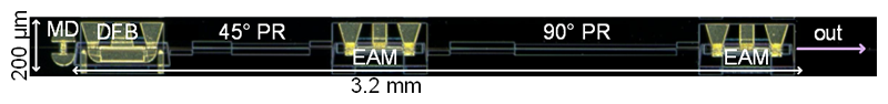
Figure 5: Image of a fabricated integrated Dual-Polarization EML device, consisting of (from left to right): a monitor photodiode (MD), a DFB laser diode emitting TE polarized light, two polarization converters, and two EAMs. The first polarization converter (45° PR) rotates the polarization by 45°, and the first EAM modulates the 50% of the laser light that remains TE-polarized. The following converter (90° PR) rotates the signal by 90° thus interchanging the TE and TM fractions. The second EAM modulates the light that was previously not modulated by the first EAM. The device was realized on HHI's PIC foundry platform.
Respective chips have been fabricated on HHI's generic PIC platform [8], and its functionality was successfully tested at 20 Gb/s per polarization state [9]. Such a chip measures only 3.2 mm x 0.2 mm. On a precursor chip without integrated laser, a total bit rate of 112 Gb/s was obtained using a baud rate of 28 GBd and PAM4 modulation [10]. By further inserting a phase shifter to modulate the optical phase between the TE- and TM-signal, a very compact transmitter for true 3-dimensional Stokes-vector modulation (SVM) could easily be implemented, delivering a bit rate corresponding to the threefold baud rate, and sixfold if additionally applying PAM4 signaling to each of the three channels. SVM represents a promising new direct modulate-and-detect technique, with a complexity and performance somewhere between direct and coherent transmission. This may have high potential for 100G access and metro networks "“to make room for some more zettabytes to come.
An alternative to electro-absorption modulators is the Mach-Zehnder modulator (MZM). MZMs exploit the quantum"“confined Stark effect which is quite efficient in InP based materials, particularly when using MQW structures. In comparison to EAMs, MZM devices build much longer (4"¦ 8 mm). This is rewarded by higher static extinction ratios (> 25 dB), operation over a wider wavelength span (~ 50 nm), and eventually probably higher electro-optic bandwidth.
As with EMLs, there is long-standing experience and expertise with Mach-Zehnder modulators on InP at Fraunhofer HHI. Already in an early development stage, a traveling-wave electrode design has been introduced to boost the bandwidth. Meanwhile, a wide range of discrete as well as integrated modulator structures of high complexity (e. g. IQ modulators) have been developed. Some of them have been transferred into commercial products by partnering with companies. Among the more recent developments is an O-band MZM that has been monolithically integrated with a DFB laser. A key step further was the co-design of the electrical driver aimed at lowest power consumption. To this end, a 2-bit digital-to-analog converter was designed for optimum impedance matching. ICs were fabricated on a 0.13 µm SiGe BiCMOS foundry platform. Fig. 6 shows a transmitter subassembly combining this IC and the DFB-MZM PIC. Tested at 56 GBd, PAM4 modulation the overall power consumption including the laser, the modulator and the driver amounted to only 332 mW [11].
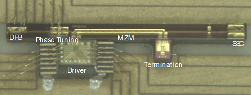
Figure 6: Co-packaged transmitter subassembly comprising the DFB-MZM chip, a 2-bit DAC driver and a load resistor. The unit was successfully tested at 56 GBd, PAM4 modulation requiring a total power consumption of only 332 mW
[1] Cisco White Paper" The Zettabyte Era: Trends and Analysis", June 7, 2017
[2] AIM Photonics Academy; "Integrated Photonics Grand Challenges and Key Needs for 2018", Webinar Dec 21, 2017
[3] M. Moehrle, H. Klein, C. Bornholdt, G. Przyrembel, A. Sigmund, W.-D. Molzow, U. Troppenz and H.-G. Bach, "žInGaAlAs RW-based Electro-Absorption-Modulated DFB-Lasers for High Speed Applications", SPIE Photonics Europe 2014, Brussels, invited paper 9134-44
[4] M. Theurer, G. Przyrembel, A. Sigmund, W. D. Molzow, U. Troppenz, M. Möhrle, "ž56 Gb/s L-band InGaAlAs ridge waveguide electro-absorption modulated laser with integrated SOA", Phys. Stat. Sol. A213, 970-974, 2016
[5] M. Theurer, H. Zhang, Y. Wang, W. Chen, L. Zeng, U. Troppenz, G. Przyrembel, A. Sigmund, M. Moehrle, and M. Schell, "2 x 56 GB/s from a Double Side Electroabsorption Modulated DFB Laser and Application in Novel Optical PAM4 Generation", J. Lightw. Techn., vol. 35, no. 4, pp. 706-710, 2017
[6] M. Theurer, M. Moehrle, U. Troppenz, H.-G. Bach, A. Sigmund, G. Przyrembel, M. Gruner, M. Schell, "ž4 x 56 Gb/s high output power electroabsorption modulated laser array with up to 7km Fibre Transmission in L-Band", J. Lightw. Techn., vol. 36, no. 2, pp. 181-186, 2018
[7] M. Baier, F. M. Soares, M. Moehrle, N. Grote, M. Schell, "Highly fabrication tolerant polarization converter for generic photonic integration technology", 28th IPRM (2016), paper MoC3-6
[8] F. M. Soares et al.," High-Performance InP PIC Technology Development based on a Generic Photonic Integration Foundry", OFC 2018, paper M3F.3 See also cover story of PIC Magazine, issue 4 (March 2017): "PICs at Fraunhofer HHI: Adding strength to InP photonic integration "
[9] M. Baier, F. M. Soares, T. Gaertner, A. Schoenau, M. Moehrle, M. Schell, "New Polarization Multiplexed Externally Modulated Laser PIC", ECOC 2018, paper submitted
[10] M. Baier et al., "112 Gb/s PDM-PAM4 Generation and 80 km Transmission Using a Novel Monolithically Integrated Dual-Polarization Electro-Absorption Modulator InP PIC," Proc. ECOC 2017, Th.1.C.4
[11] S. Lange et al., "Low Power Optical Transmitter with DFB-Laser Mach-Zehnder Modulator PIC and Co-Designed 2-Bit DAC Driver," Proc. ECOC 2017, Th.1.C.5


