
Dots and wells deliver lasing on silicon
Spurring the development of silicon photonics is the world’s first InP-based laser grown on exactly orientated silicon
BY KEI MAY LAU AND YU HAN FROM HONG KONG UNIVERSITY OF SCIENCE AND TECHNOLOGY
We are living in a zettabyte era, where digital data is generated, processed, stored, and transmitted at unprecedented rates. Demand for data is only going to increase, and satisfying this will not be easy. However, it can be fulfilled by silicon photonics, drawing on cost-effective microelectronics technologies to realize ultra-high-bandwidth, power-efficient photonics on the traditional silicon platform.
An essential but elusive component for silicon photonics is a compact, efficient, on-chip semiconductor light source. For the past decade, the development of this source has focused on heterogeneous integration – that is, the bonding of conventional III-V semiconductor laser dies onto silicon photonic wafers. This hybrid integration technique is not as attractive as monolithic integration, involving the direct growth of III-V lasers on silicon. But realising the latter is more challenging, partly because in order to ensure compatibility with present IC technology, lasers must be integrated on CMOS-standard (001)-oriented silicon substrates without an offcut. The offcut (mis-orientation) was deemed necessary to overcome the anti-phase boundary defects formed when growing polar semiconductors (III-V) on non-polar silicon. What’s more, as the ICs will be used in data communications, these lasers must operate at telecommunication wavelengths – the 1.3 µm and 1.5 µm band. And if this approach is to be commercially successful, the lasers that are produced must deliver a high performance, and be coupled with other silicon photonics components in a scalable, cost-effective manner.
At Hong Kong University of Science and Technology, we can address most of these concerns with a technology that enables direct hetero-epitaxy of III-V coherent lasers on silicon substrates. This approach, involving MOCVD, offers the potential for lower cost, higher yield, and scalability than chip-scale bonding.
One of the challenges of direct growth is how to address the polarity and lattice mismatch between the III-Vs and silicon. Crystalline defects emerge from the III-V/silicon interface, including various kinds of dislocations, and they can jeopardize laser performance and reliability. Special techniques are required to suppress the generation and propagation of these dislocations, and enable efficient light emission on silicon substrates. We are pioneering one promising solution, based on low dimensional In(Ga)As quantum structures. By embedding quantum dots inside optimized InP buffer layers that are grown on silicon substrates, we are able to use MOCVD to produce 1.5 µm-band InP-based lasers on industry-standard silicon wafers.
Quantum dot lasers on silicon
Fabrication of our lasers begins with the growth of III-V alloys on 300 mm nano-patterned silicon wafers. This involves a unique patterned growth process on exact (001)-oriented silicon substrates, rather than 2-6° offcut silicon, the platform adopted by many other groups (see Figure 1(a)). Our efforts begin by creating [110]-aligned oxide trenches atop the silicon wafer. Anisotropic wet etching follows, to obtain densely packed V-shaped pockets with two concave, atomic-sharp {111} surfaces. By nucleating GaAs inside these nano-pockets, we eliminate the formation of anti-phase boundaries – a crystalline defects that is detrimental to devices. We find that GaAs nanowires first nucleate inside the nano-pockets that coat the {111} surfaces. Continued growth leads to the coalescence, creating thin films. Thanks to the unique tiara-shape of the nano-pockets, we find that the planar defects generated at the interface of GaAs and silicon are unable to propagate into the above heterostructures (see Figure 1(c)).
Our next step is to grow an InP layer on the coalesced thin film of GaAs. Due to the 4 percent lattice mismatch between InP and GaAs, dislocations appear at the interface between these two materials. To prevent them from propagating into device regions, we insert ten periods of In0.6Ga0.4As/ InP strain layer superlattices inside the InP buffer. The strain inside these superlattices changes the propagation direction of the dislocations, causing them to either annihilate or propagate to the edge of the sample (see Figure 1(b)).
We have scrutinised the quality of our material with transmission electron microscopy. This reveals a defect density of 1.5×108 cm-2, which is one of the lowest values reported for an InP thin film grown on silicon (see Figure 1(d)). We believe this is not the limit, and are currently exploring new methods to further reduce the defect density.
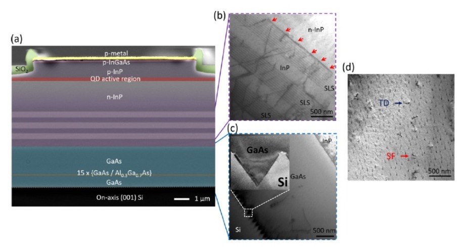
Figure 1. (a) Colour-enhanced cross-sectional scanning electron microscopy image of the whole epitaxial structure after laser fabrication. (b) Cross-sectional transmission electron microscopy images of three stacks of a 10-period InGaAs/InP strain-layer superlattices with dislocation filtering effects identified by red arrows, (c) 2.2 µm-thick GaAs intermediate buffer on a nano-patterned V-grooved on-axis (001) silicon substrate; inset shows the defect trapping effect of the tiara-shaped pocket enclosed by {111} facets. (d) Plan-view transmission electron microscopy characterization of defect density of the InP buffer on silicon.
On this foundation we deposit several layers of quantum dots. These nanostructures, which support strong quantum confinement and have a delta-function-shaped density of states, promise to enhance laser performance, in terms of lasing threshold, maximum modulation frequency and temperature stability. What’s more, quantum dots have a superior tolerance to dislocations, thanks to a three-dimensional confinement of charge carriers. This fine set of attributes make an array of quantum dots the ideal choice for the active gain medium for lasers grown on silicon.To see if they can fulfil their promise, we have embedded five layers of InAs quantum dots inside a laser structure on the InP buffer. Each of the layers of dots, formed using the Stanski-Krastanow growth mode, is capped with two layers of optimised InAlGaAs spacers. They have a thickness that has been carefully tuned to ensure a strong, narrow photoluminescence spectra.
Atomic force microscopy reveals that our samples have a quantum dot density of 4.5 × 1010 cm-2 (see Figure 2 (a)). This technique has also evaluated the flatness of the surface of the full laser structure. It has a surface roughness of just 1.4 nm (Fig. 2(b)). Meanwhile, photoluminescence measurements produce a strong peak centred at the 1.5 µm band (see Figure 2(a)).
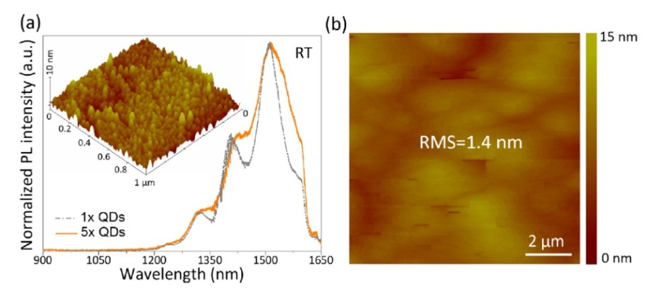
Figure 2. (a) Normalized room-temperature photoluminescence spectra of 1 and 5 layers of quantum dot active regions grown on silicon. Inset shows an atomic force microscopy image of the top layer quantum dots with a dot density of 4.5 × 1010 cm-2. (b) Atomic force microscopy image of the as-grown quantum dot laser on silicon, showing a smooth surface with a root-mean-square value of 1.4 nm.
We have used this heterostructure to produce the world’s first electrically injected 1.5 µm quantum dot laser that is directly grown on silicon. This success has hinged on combining our low-defect InP templates with optimized InAs quantum dots. These lasers, in the form of Fabry-Pérot bars, have end-facets formed by cleaving, and dimensions of 5 mm by 10 µm. Driving these devices with pulses produces a room-temperature output power in excess of 110 mW. The threshold current density is 1.6 kA cm-2, equating to 320 A cm-2 per quantum dot layer. Operation is possible up to 85 °C, and the characteristic temperature is 59 K (see Figure 3).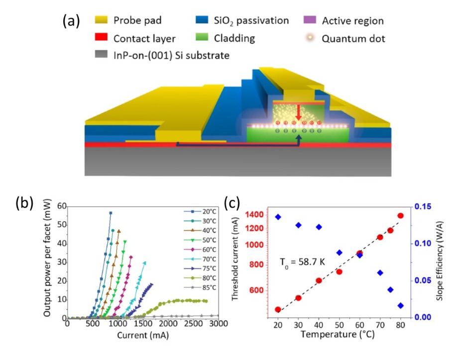
Figure 3. (a) Schematic of an InAs/InAlGaAs/InP quantum dot laser on silicon substrates. (b) Light output power versus current for a 20 µm × 1000 µm device at various temperatures. (c) Threshold current and slope efficiency change as a function of temperature. The characteristic temperature is extracted to be 58.7 K.
This result is an important step towards our goal of equipping silicon photonic chips with efficient light emitters, in the form of high-performance 1.5 µm quantum dot lasers directly grown on silicon. Right now, we are targeting continuous-wave operation, a goal that we hope to accomplish by reducing the dislocation density of the InP-on-silicon template, improving the quantum efficiency of InAs quantum dots, and optimising the overall laser structure.
Lasers at the nano-scale
Our efforts have also focused on the direct epitaxy of 1.5 µm InP-based nano-lasers on silicon substrates. Like the scaling of silicon transistors, as governed by Moore’s Law, the shrinking of the laser footprint to nanometre scale delivers several benefits. In this case it cuts energy consumption, while increasing the integration density of silicon photonic integrated circuits.
The starting point for the creation of our nano-lasers, featuring InP nano-ridges, is nano-patterned, (001)-oriented, silicon-on-insulator (SOI) substrates. Using the aspect ratio trapping technique, we begin by depositing an ultra-thin GaAs wetting layer – it is around 10 nm-thick – at the {111} silicon surface, to facilitate subsequent InP nucleation. With this approach we can confine most of the crystalline defects within the III-V/silicon interface, due to the unique strain-relaxing mechanism (see Figure 4(b)).
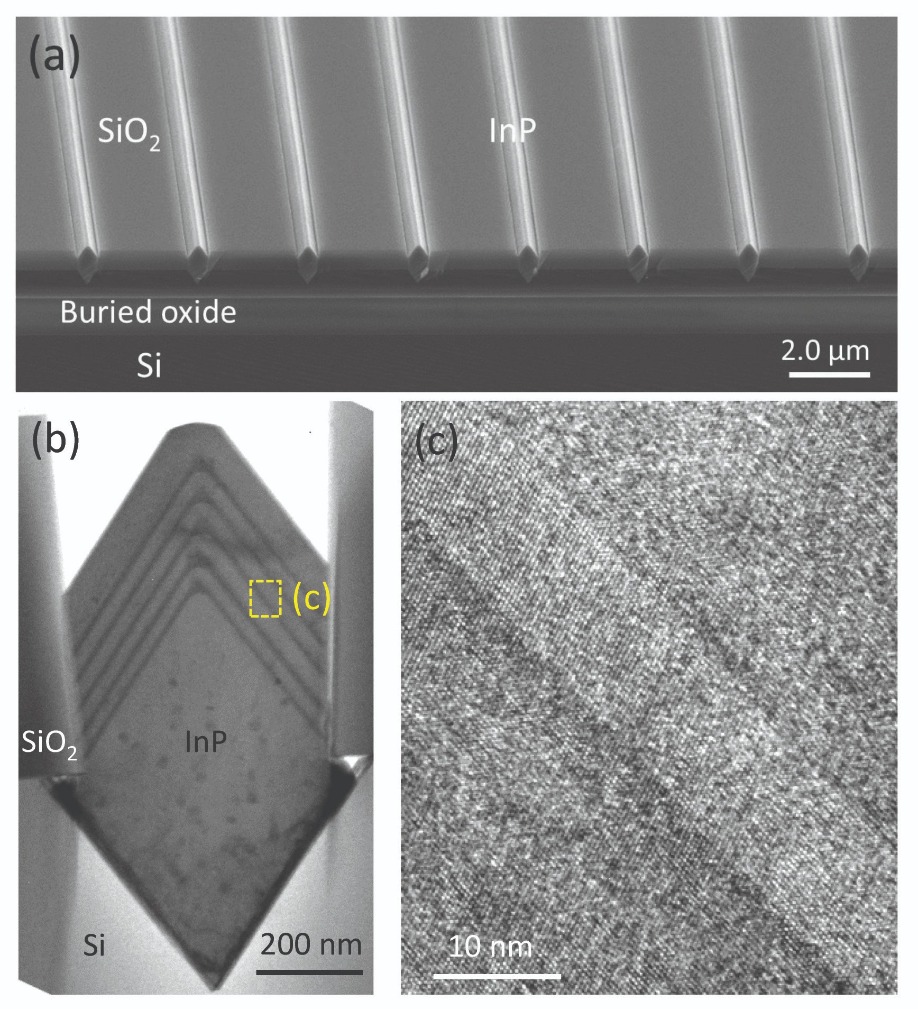
Figure 4. (a) Scanning electron microscopy image of the highly ordered, in-plane InP/InGaAs nano-ridge structures on (001) silicon-on-insulator wafers. (b) Cross-sectional transmission electron microscopy image of the InP/InGaAs nano-ridge perpendicular to the wire, showing five {111} ridge InGaAs quantum wells embedded inside an InP nano-ridge; the dark area at the InP/silicon interface contains a high density of stacking faults generated for strain relaxation. (c) High-resolution transmission electron microscopy image of one InGaAs ridge quantum well with atomic sharp InP/InGaAs interfaces.
The resulting as-grown InP nano-ridges, which have a width of 450 nm and a height of 1.0 µm, develop a convex growth front. Two large {111} facets and one tiny (001) facet form inside the oxide trenches. This lack of uniformity is a nuisance, complicating the insertion of lattice-matched InGaAs quantum structures. That’s because the ternary InGaAs alloy tends to exhibit different chemical compositions at different facets. Due to this compositional inhomogeneity, the photoluminescence spectra is broad and multi-peaked.Our solution is cycled growth. This allows us to manipulate the distribution of InGaAs on the multi-faceted InP ridge buffer at a single-atomic-layer level. As a result, we can grow InGaAs quantum wells with atomic sharp interfaces and superior optical properties (see Figure 4(c)).
One of the key challenges with nano-lasers on silicon is the confinement of the optical modes within the sub-wavelength nano-cavities. We improve the confinement with a hybrid InP/InGaAs Fabry-Pérot nano-cavity design that is supported by silicon pedestals (see Figure 5(a)). The silicon pedestal is formed via anisotropic wet etching, with the dimensions carefully controlled to ensure both strong optical confinement inside the nano-ridge and robust mechanical support for the top laser cavity (see
Figure 5 (b) and 5 (c)). The silicon pedestal, which features atomically sharp {111} surfaces, could also serve as a low-loss waveguide. This structure could couple light from the laser cavity above, providing potential on-chip light manipulation.
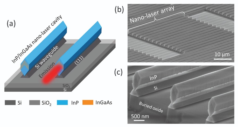
Figure 5. (a) Schematic of the designed InP/InGaAs nano-laser array grown on an SOI substrate. (b) Tilted-view scanning electron microscopy image of the InP/InGaAs nano-laser array on SOI. (c) Zoomed-in scanning electron microscopy image of the end-facets of the nano-laser array.
In sharp contrast to the commonly reported vertical nanowire lasers – they have a cavity length that is governed by the growth parameters and is normally shorter than 10 µm – our horizontally-aligned InP nano-cavity, which is defined by lithography, has a length that can vary from a few microns to hundreds of microns. Another merit of our technology is that thanks to the in-plane configuration of nano-lasers on SOI wafers, our devices can be integrated with other silicon-based photonic components, including waveguides, splitters and (de)multiplexers that are also processed on SOI substrates.Optical pumping
Measurements on our laser with a 60 µm cavity reveal that optical pumping produces room-temperature lasing in the 1.5 µm band. Under low excitation, the output from the nano-laser combines broad spontaneous emission with well-spaced Fabry-Pérot resonance peaks. Crank up the pumping, and a 1518 nm peak protrudes from the background emission, before lasing kicks in. Far above threshold, the intensity of the 1518 nm single-lasing-mode is orders of magnitude higher than the clamped background emission. Further support for lasing is the apparent threshold behaviour in the plot of output with pump power, and the line-width narrowing of the emission peak (see Figure 6(b)).
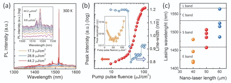
Figure 6. (a) Room-temperature emission spectra around threshold. Inset shows the emission spectra plotted in a logarithmic scale. (b) The evolution of the peak intensity and the line-width as the excitation level increases. Inset presents the progression of peak position as a function of pumping levels. (c) The relationship of the lasing peak and the length of the nano-cavity.
By varying the length of the cavity, we can produce lasers with different emission wavelengths from the same epiwafer. For example, increasing the length of the cavity from 40 µm to 60 µm can shift the dominant lasing mode from 1400 nm to 1550 nm.This correlation between the lasing mode and the cavity length stems from the wavelength-dependent modal gain and propagation/end-facet loss. As a longer wavelength leads to a larger round-trip loss and a smaller modal gain, a larger volume of active material is needed to reach threshold. The opportunity to tune the lasing wavelength over multiple telecom bands suggests that our technology could serve in compact wavelength-division multiplexing systems.
Our incorporation of a telecom nano-laser array onto CMOS-compatible, (001)-oriented SOI substrates highlights the feasibility of on-chip integration between compact III-V nano-scale light sources and mature silicon photonic components. Aiming at developing nano-scale photonic integrated circuits on SOI, we are now focusing on the design of electrically driven nano-lasers on SOI wafers. Look out for our future publications, as we are confident that we will soon have more promising results to report.
Q. Li et al. Appl. Phys. Lett. 106 072105 (2015)
S. Zhu et al. Appl. Phys. Lett. 113 221103 (2018)
Y. Han et al. Appl. Phys. Lett. 108 242105 (2016)
Y. Han et al. Optics Letters. 44 767 (2019)


