
Building better lasers on low-cost silicon

The silicon photonics revolution is gathering pace, thanks to the introduction of powerful lasers that don’t require an insulating intermediary layer
BY DONGJAE SHIN AND KYOUNGHO HA FROM SAMSUNG ADVANCED INSTITUTE OF TECHNOLOGY, SAMSUNG ELECTRONICS
Back in the middle of the twentieth century, a revolution took place in the electronics industry. Out went the vacuum tube and in its place came the integrated circuit.
Now this industry is starting to embark upon another major change. There is a shift to the optical domain, driven by scalability limitations associated with some electric ICs, along with the promise of newly emerging applications. To usher in this new era, money is pouring into silicon photonics technology, enabling the integration of photonic devices.
Part of the motivation behind this investment is that there are several applications where the addition of photonic ICs could aid ‘mother’ electric ICs. They include CPU-memory interconnects, an opportunity that has been discussed for several decades.
Introducing inter-chip optical interconnects could obliterate bandwidth and capacity limitations coming from today’s copper interconnects, which are hampered by impedance mismatches between the CPU and the dual-inline memory modules. This could create a form of DRAM with an optical interface, formed by integrating silicon-photonics-based optical transceivers in the DRAM on the bulk-silicon platform (see Figure 1).
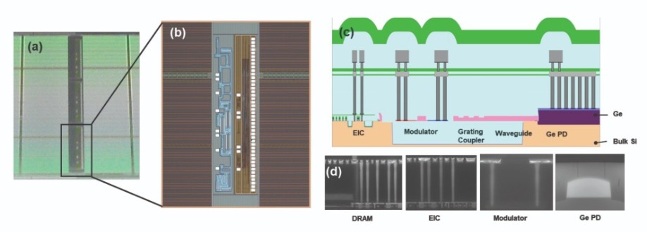
Figure 1. (a) Optical microscope image of a DRAM periphery section. (b) Optical microscope image of the electric-photonic IC. (c) Schematic of the electric-photonic IC vertical structure. (d) Scanning electron microscopy images of the DRAM, electric IC, modulator, and germanium photodiode. Note that this approach, outlined by Samsung in 2013, did not include the integration of lasers.
This vision does not quite align with the majority of effort within the silicon photonics industry, which has focused on a special integration platform called silicon-on-insulator (SOI). This platform simplifies and speeds development, but has a fundamental flaw:it is incompatible with conventional general-purpose substrates, known as bulk-silicon, that are used for most legacy electrical ICs. While there is no question that SOI is convenient for implementing photonic ICs at an early stage, it is likely to be a stumbling block to the evolution of electric-photonic ICs.
For this reason, at Samsung Advanced Institute of Technology, we are pursuing photonic IC technology on bulk silicon. Our breakthrough is the development of integrated lasers, implemented with a direct bonding process on the bulk-silicon platform. Our success provides a small but significant step towards the integration of photonic functions into legacy high-volume products, and it could contribute to mainstream semiconductor product evolution.
It makes sense for some smaller companies to develop their photonic technology on SOI, because the size of the emerging market for their technology is large enough for them. But for those of us that are players in the major semiconductor industry, which is already mass-producing electric IC products, the focus tends to be on the electric-photonic ICs. It is this technology that could support the electrical IC market of the future (see Figure 2).
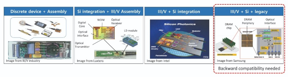
Figure 2. The photonics industry is pursuing several different approaches to unite III-V and silicon technologies. For the last stage of the integration with legacy technologies, photonics integration needs backward compatibility with the legacy platform.
The pace of development of silicon photonics that are based on the bulk-silicon platform has been slower than that on SOI. However, there has been progress on bulk-silicon, and the main device library is now almost complete.On the bulk silicon platform, developing the integrated laser is the biggest challenge. This building block, like all photonic devices on bulk silicon, suffers from a relatively high optical loss compared with the SOI platform. However, bulk silicon also has its upsides, including a lower cost and a superior heat dissipation that improves laser performance. It is these merits that give the implementation of electric-photonic ICs so much promise.
SOI versus bulk silicon
Despite a cost that is an order of magnitude higher than that of bulk silicon, SOI substrates are firmly established as the mainstream platform for silicon photonics, due to their ease of fabrication, and the low optical loss of the optical waveguides. At the heart of this technology is a global intermediary layer called a buried oxide. It sits beneath the thin crystalline silicon layer, where it creates a low-loss optical waveguide, by surrounding the high-index crystalline silicon core with a low-index oxide cladding. The downside of this architecture, as mentioned before, is its heat dissipation – the thermal conductivity is two orders of magnitude lower than that of silicon.
As this bulk-silicon platform is far lower in cost, and is currently used in most high-volume IC products, it is likely to be used in future electric-photonic ICs. With this platform, it is possible to add a buried oxide locally, under just the optical waveguide. This can impede light leakage, as well as increasing heat dissipation to the substrate, a move that prevents a plummet in the performance of temperature-sensitive devices.
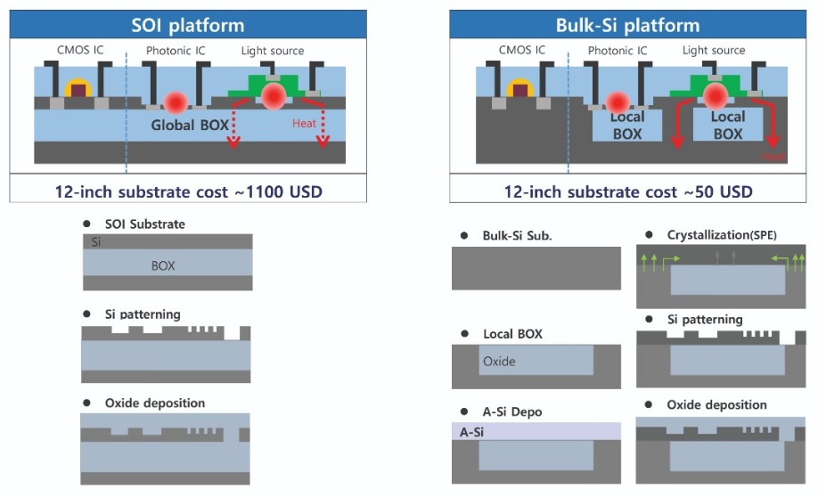
Figure 3. Despite its high-cost substrate, the SOI platform has been dominant in the photonics industry. Merits of the bulk-silicon platform include its low-cost substrate, and its attractiveness for forming electric-photonic ICs. A noteworthy difference between the two architectures is that the SOI platform features a global buried oxide (BOX), while the bulk-silicon platform employs a local BOX.
One of the challenges with bulk-silicon technology is realising a layer of low-loss crystalline silicon on top of the amorphous buried oxide. Recently, however, we have made much progress on this front, using heat treatment to crystallise the amorphous silicon that has been deposited on the buried oxide. Although the optical waveguide loss for the crystallised silicon on the bulk-silicon platform is higher than that for crystalline silicon for SOI, it is still low enough to serve in photonic ICs with relatively short optical waveguides.Integrating III-Vs with silicon
As silicon lasers are still in their infancy, the lasers that are deployed in silicon photonics have to be made from III-Vs. The goal is to ensure low-cost coupling between the III-V laser and the silicon chip. Many solutions have been proposed, ranging from packaging-level assembly to process-level integration. With the assembly approach, the challenge is to realise high-precision optical alignment at low cost, while integration is held back by the substantial investment required to set up integrated processes for handling heterogeneous materials.
Once again, the approach that is adopted is dictated by the size of the industry. If it is small, the preference is on assembly, which provides a swift response to the emerging market; but if a company is operating in the major semiconductor industry, its interest lies in integration, with greater focus on high-volume manufacturing. Turning to integration avoids unacceptable increases in packaging costs, which are forbidden in the major semiconductor industry.
The bonding process is a popular short-term approach to integrating III-Vs and silicon. It overcomes the difference in the lattice constants of heterogeneous materials. Epitaxial layers of III-Vs are grown on a native substrate, before this epiwafer is flip-chip bonded to a silicon substrate that features pre-patterned silicon photonics structures. After the bond has been strengthened with a heat and pressure process, integrated lasers are formed using photolithography and III-V processing. The accuracy provided by lithography eliminates additional alignment.
Unfortunately, the scale and the maturity of silicon and III-V processes are very different. Consequently, integrating them is hampered by various technical and business issues, which may only be addressed with engagement of the overall semiconductor industry.
When pursuing this approach to integration, the first hurdle is to develop a good enough bonding process. Options include buffered bonding and direct bonding (see Figure 4). The former has fewer challenges, but the later delivers a simple silicon-to-III-V connection with diminished wavelength dependency.
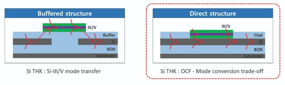
Figure 4. The two main options for bonding are buffered bonding and direct bonding. The buffered structure takes full advantage of the traditional III-V active design and focuses on the smooth laser-waveguide mode transfer. The direct structure relies on an active design that depends on the III-Vs and silicon, and is capable of realising smooth laser-waveguide mode conversion. The thickness of the silicon plays an important role in mode transfer or mode conversion.
From a thermal perspective, direct bonding is better, because silicon tends to have a higher thermal conductivity than the buffer layer. Given the great thermal management associated with the bulk-silicon platform, it appears to be worthwhile to maintain this asset when bonding. Refining the process, so that it is well-suited to high-volume manufacture, is a goal for those that work in research and development.Building lasers on bulk silicon
With the bulk-silicon platform, a crystallized silicon layer must be formed on top of the local buried oxide. We do this with our proprietary solid phase epitaxy process. Essentially, this is a form of mild thermal annealing that turns amorphous silicon to crystalized silicon that mirrors the crystalline seed of the substrate. The crystallinity of the substrate propagates upwards in the regions directly contacting the amorphous layer, and propagates sideways over the local buried oxide.
Note that for the silicon at the centre of the local buried oxide, crystallization propagates from both sides – and when they collide, the result is poor crystallinity, known as coalescence. To prevent this poor crystal quality from impairing the performance of the optical waveguide, its location deliberately avoids the coalescence regions.
Putting aside for one moment the use of a local buried oxide and the offset location of the optical waveguide, we employ a process and structure that are similar to the SOI platform. However, our approach offers some advantages over this in terms of flexibility, as we can use arbitrary thicknesses for the silicon layers, the buried oxide, and the polysilicon reflective layers.
The most common method for getting the output of a discrete laser into a waveguide is butt-coupling. This is accomplished by aligning the laser and the waveguide on the same optical axis. In this configuration, the optical mode is positioned at the centre of the laser active region to maximise efficiency.
In this regard integrated lasers are very different, due to the evanescent coupling. The III-V active region is attached to the top of the silicon waveguide, allowing the evanescent tail of this device’s emission to couple with this waveguide. Due to this unique feature, the optical mode is not at the centre of the integrated laser, but distributed over both the III-V and the silicon structures.
With this design, the silicon waveguide provides a resonating cavity structures to the optical mode, and the III-V active region provides optical gain to the optical mode. It is this interplay of the gain and cavity, and how the optical mode is distributed over the silicon and III-V regions, that governs the performance of the integrated laser. For example, if the optical mode is primarily in silicon, this trims the internal loss, cavity loss, and laser-waveguide coupling loss, but at the expense of a reduction in optical gain from the III-V active region. Since the ratio of the optical mode in the III-Vs to that in silicon is determined by the waveguide dimensions, as well as the structure and the thickness of the III-V region, laser development cannot ignore the interplay of the silicon and III-V structures.
Like III-V discrete lasers, if integrated lasers are to work well, the electrical currents must be concentrated in the optical mode. To do this, we use a proton implant process to make the III-V mesa edges non-conductive (see Figure 5). The proton-implanted regions actually serve two purposes: they act as a funnel for current concentration, and they aid the transfer of heat from the active region to the silicon layer. Current is vertically injected into the optical mode from the p-type electrode that sits on top of the III-V mesa, and then it flows in the horizontal direction to drain into the n-type electrode.
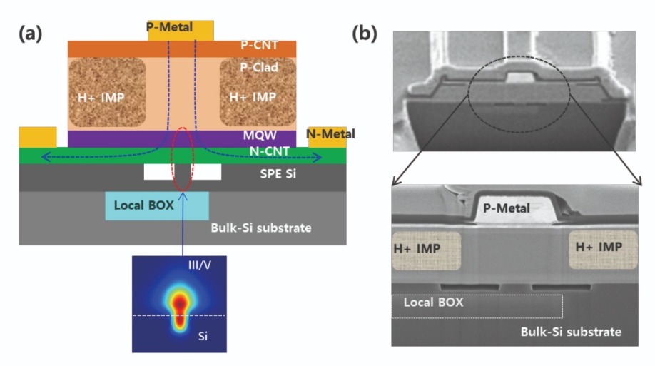
Figure 5. The integrated laser on the bulk-silicon platform includes: a III-V epitaxial layer directly bonded to the pre-patterned silicon wafer; current confinement, realised with the proton-implanted III-V mesa structure; and optical confinement, resulting from the III-V mesa on top of the silicon rib waveguide. Note that to minimise optical loss, there is the lateral offset between the local buried oxide (BOX) structure and the rib waveguide.
Optimising the performance of this laser is not easy, due to the interplay of various characteristics. One option to increase the laser efficiency is to shorten the current path, which cuts electrical resistance. But if a low thermal impedance is also required, accomplishing this by widening the III-V mesa and lengthening the horizontal current path, leads to a higher electrical resistance and a lower laser efficiency.Tuning the wavelength?
Depending on the application, the photonic IC may require a laser that emits a single-wavelength or one with a tuneable output. This difference lies in the cavity structure in the silicon side of the integrated laser.
For single-wavelength lasers, the most popular design is the distributed feedback laser (see Figure 6 (a)). By forming a cavity at a single wavelength through a specific grating structure, emission is restricted to a single mode, regardless of driving conditions.
The key metrics for the single-wavelength laser are the wall plug efficiency and the side-mode suppression ratio, which is a measure of the dominance of the lasing mode. In a typical III-V laser, the wall plug efficiency falls as the temperature of the device increases, due to reductions in the gain and the bandgap of the III-V material. In the integrated laser, the situation is more complicated. The thermal behaviour of the silicon must also be considered, and whether its pairing with the III-Vs can apply the brakes to the reduction in wall-plug efficiency with temperature. We have strived to improve the performance of our integrated lasers. This has led us to realise a single-port wall-plug efficiency of 8 percent up to 70 °C and a side-mode suppression ratio of 45 dB (see Figures 6 (c) and (d)).
Several designs are capable of producing a wavelength-tuneable laser. Our device is based on a popular design that features two ring-based mirrors (see Figure 6 (e)). The range of tuning can be broadened with laser mode hopping through the Vernier effect.
With this class of laser, the range of tuning is paramount. Using a proper ring design, we have produced a tuning range of 42.2 nm on the bulk-silicon platform (see Figure 6 (g) and (h)).
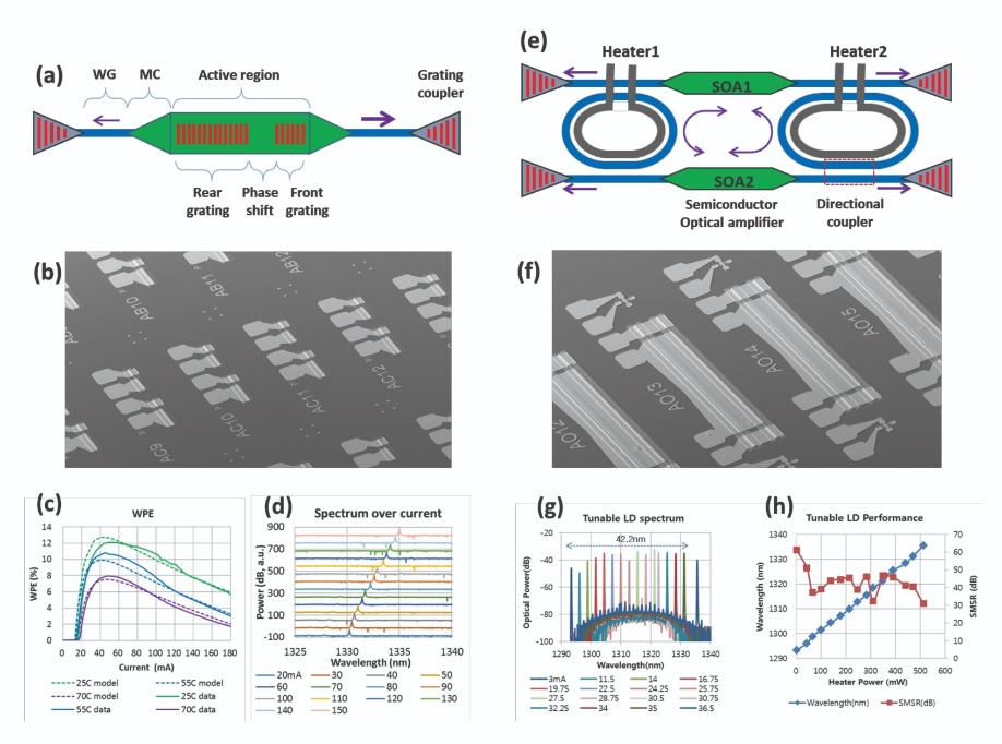
Figure 6. Engineers at Samsung Advanced Institute of Technology have used a bulk-silicon platform to produce and evaluate single-wavelength integrated lasers (see (a) to (d)), and wavelength-tuneable integrated lasers (see (e) to (h)). The single-wavelength laser is a distributed feedback design that realises a high side-mode suppression ratio, and features a quarter-wavelength phase-shift section in the distributed feedback grating (a). Note that this short phase-shift hampers a high wall-plug efficiency, but guarantees single-mode stability. In the integrated lasers, thanks to fine tuning of the design and high precision of the silicon process, it is possible to suppress the deterioration of the mode stability in a longer phase-shift design. To enhance the main-port optical output, the design incorporates an asymmetric cavity structure with different grating lengths on both sides of the phase shift. The wavelength-tuneable laser features a ring-based mirror, with the ring resonator inserted between the two straight waveguides (e). With an optical input to one waveguide, the other waveguide outputs the so-called wavelength comb according to the input wavelength. The result is a mirror-like operation at the selected resonant wavelengths. Note that the ring size determines the wavelength comb periodicity. So, with two rings of different sizes, each ring mirror reflects only at the wavelength comb of a different periodicity. This means that the laser cavity is formed only at the wavelength where the two wavelength combs overlap. If one wavelength comb is then spectrally shifted by the embedded heater of the ring, this action will shift lasing to the adjacent mode in the wavelength comb. (b) and (f) are scanning electron microscopy images of the single-wavelength and tuneable integrated lasers, respectively. (c) Wall-plug efficiency of the single-wavelength laser at 25°C, 55°C, and 75°C. The continuous lines are measurements, and the dotted lines are from a laser model. (d) Optical spectra of the single-wavelength laser, driven at operating currents from 20 mA to 150 mA. (g) Optical spectra of the wavelength-tuneable laser, for a range of heater currents. (h) Lasing wavelength and side-mode suppression ratio extracted from the optical spectra.
Thermal advantageWe have evaluated the thermal advantage of our bulk-silicon platform by measuring the thermal impedance of our single-wavelength integrated laser. The thermal impedance is defined by the ratio of the temperature change of the laser’s active region, relative to its input electrical power. The greater the heat dissipation, the smaller the impedance. We have found that moving from an SOI integrated laser to one that is on bulk silicon cuts thermal impedance by about 40 percent, assuming no change in the length of the device.
To evaluate the impact of this improvement in thermal impedance on laser performance, we have turned to a measurement-calibrated theoretical model. Based on this insight, at 70 °C we predict that compared to the SOI platform, the use of bulk-silicon enables a 52 percent hike in the maximum optical output power and a 13 percent increase in the wall plug efficiency (see Figure 7). And if we were to thin the substrate, the resulting reduction in thermal impedance could increase the maximum optical output power at 70 °C by more than 140 percent. Based on this modelling, the bulk-silicon platform is particularly promising for electric-photonic ICs that require either many temperature-sensitive devices or high-power lasers.
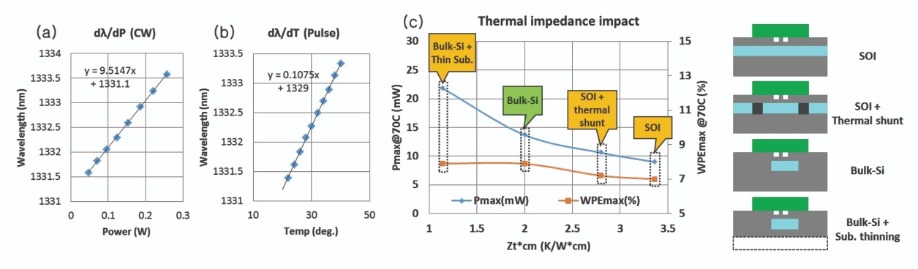
Figure 7. Thermal analyses of the single-wavelength laser on the bulk-silicon platform. It is challenging to undertake direct measurements of local temperature change in the active region, so this characteristic is indirectly measured through lasing wavelength change. Rates of lasing wavelength change are measured in terms of temperature and input power, with the ratio of these two revealing the thermal impedance. (a) Lasing wavelength shift over increasing power in continuous operation. (b) Lasing wavelength shift over increasing temperature, using pulsed excitation with a 0.1 percent duty cycle. (c) The maximum output power and the maximum wall-plug efficiency at 70 °C, calculated using the laser model for the four platforms of interest. The calculation is calibrated with the measured data of the bulk-silicon platform.
Addressing reliability concerns Due to the significant difference in the thermal expansion coefficients for silicon and the III-Vs, there are concerns related to the reliability of integrated lasers. On the SOI platform, a typical reported value for the average lifetime at 70 °C is about 40,000 hours. That’s slightly shorter than the average lifetime of our lasers on bulk-silicon. They have a lifetime of about 46,000 hours at 70 °C (see Figure 8).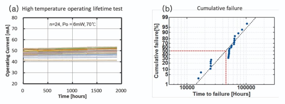
Figure 8. (a) A high-temperature operating lifetime test, conducted at 70°C, run over 1900 hours with 24 single-wavelength lasers. The output power was set to 6 mW. (b) The cumulative failure plot provides an estimate for device lifetime.
Is this long enough? Well, due to the difficulty of optical fibre deployment, conventional long-distance fibre systems typically require long-term reliability of more than 10 years – or nearly 90,000 hours. However, recently constructed data centres adopt a crop-rotation-like replacement of optical interconnect modules, deploying new product every three to four years. So, for applications such as data centres, where long-term reliability is not essential, our lasers show much promise.Dongjae Shin et al. “Heterogeneously integrated light sources for bulk-silicon platform,” IEDM2018, 23.6 2018
Dongjae Shin et al. “Integration of silicon photonics into DRAM process,” OFC 2013, OTu2C 2013


