After 30 years, PIC Honoree Graham Reed and CORNERSTONE are Just Getting Started
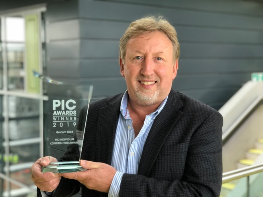
Silicon photonics pioneer Graham Reed was honored with a 2019 PIC Award for individual contributions to the industry he helped create. While Reed accepts the accolades, he is quick to point out that his accomplishments, and the CORNERSTONE programme at the University of Southampton, have been and always will be a team effort.
New applications and markets regularly emerge for silicon photonics (SiP) and related technologies that have been foundational to the development and evolution of photonic integrated circuits (PICs). Pioneering individuals and companies they founded recognized the potential of utilizing low-cost silicon fabrication techniques and processes for optical and digital data applications. Their work revolutionized ‘business as usual’ and along the way they created an industry.
What was not too long ago seen as an emerging technology is now at work in datacenters and telecom networks as part of transceiver modules and switches or playing key roles in other digital data components. The performance gains, size reductions and power savings of using photons in place of electrons to transmit and receive data continues to grow.
Professor Graham Reed, University of Southampton, was honoured with a 2019 PIC Award for individual contributor accomplishments. Speaking with Reed after the awards were presented at the PIC International Conference in Brussels, he noted that although the PIC Award is tied to his pioneering silicon photonics (SiP) work, and in particular the CORNERSTONE project, the field itself and core photonic integration technologies grew as collaborative efforts utilizing II-VI / III-V materials and fabrication technologies.
“When I started in this area, it wasn’t even called silicon photonics…we called it integrated optics in silicon, but what the name meant was actually that silicon was primary, and not much else was present besides some germanium used in the detector. We were thinking of sensor networks for the first application, and those are now coming about. But almost from the start the field involved integration, like the light source, which brought in III-V materials. And today we are looking at all sorts of materials, modulation schemes and ways you can combine polymers into different sorts of waveguides. So when you consider how the field has grown and changed today, a better name might be silicon compatible photonics,” he said.
Reed has dedicated much of his professional career to developing devices that today play a pivotal role in the growing photonics integration industry. He established the first Silicon Photonics Research Group in 1989 at Surrey, later moving programme components to Southampton. A noteworthy outgrowth of his early work was the establishment of the first silicon photonics company, Bookham Technology, which was led by former student, Dr. Andrew Rickman, now CEO of Rockley Photonics. Bookham is now part of Lumentum Holdings, a leading supplier of integrated photonics products to telecom and datacom networks. Amongst many accomplishments in silicon photonics, Reed’s team pioneered the pre-emphasis technique; the first 1 GHz modulator design and the first depletion modulator design that evolved into an industry standard. The team also pioneered industry-leading efforts that include creating the first 40GB/s modulator with high extinction ratio; the first 40Gb/s polarisation independent modulator; the first slow wave modulator, and the first 50Gb/s modulator.
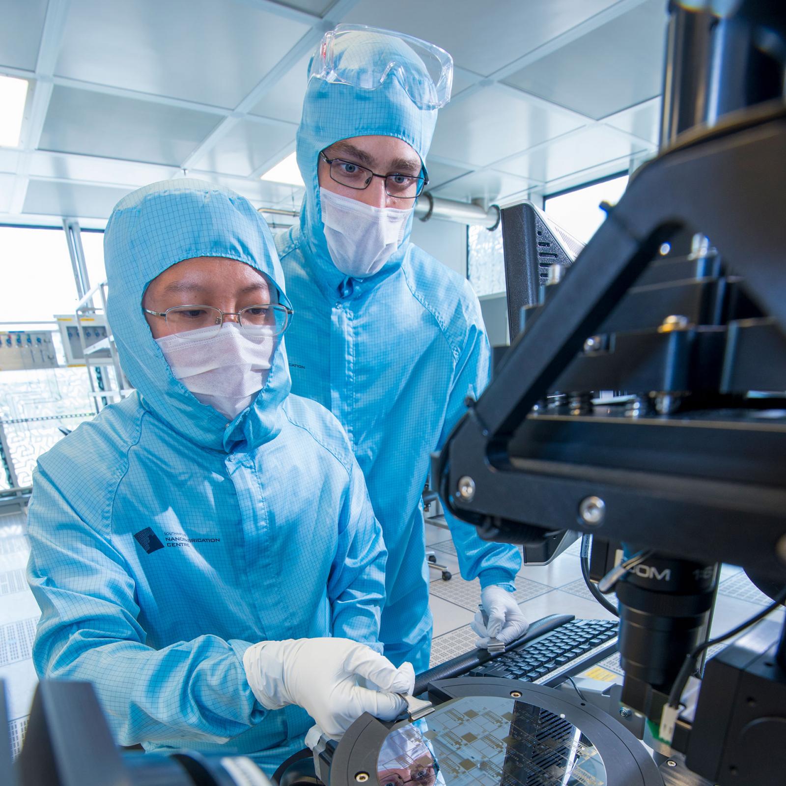
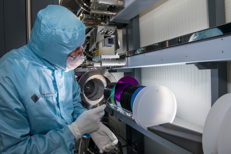
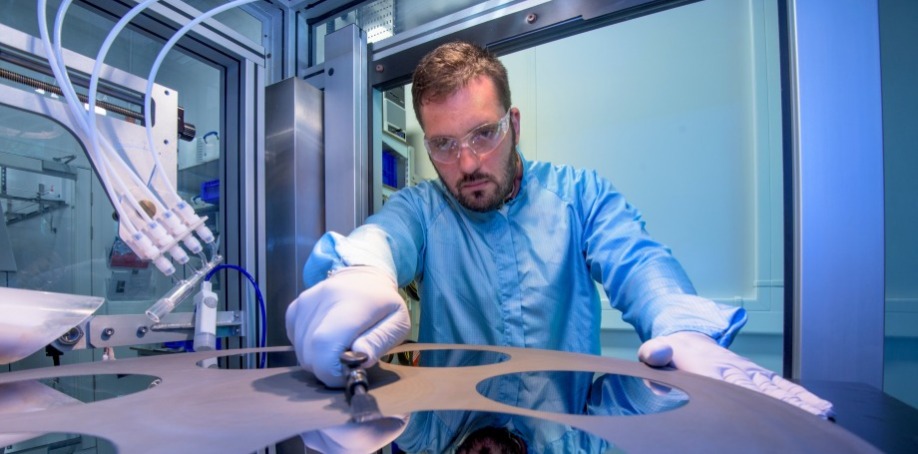
Reed is presently the Deputy Director of the Optoelectronics Research Centre (ORC) at Southampton and Director of CORNERSTONE—a rapid prototyping, multi-project wafer (MPW) programme also housed at Southampton that benefits companies and researchers developing new photonic integrated circuits (PICs). The CORNERSTONE project is funded by the Engineering and Physical Sciences Research Council (EPSRC) and is part of collaborative photonics research and manufacturing development programmes in the UK involving universities at Glasgow, Southampton and Surrey. Device fabrication at wafer scale is conducted primarily in Southampton’s ORC cleanrooms, and at chip scale in Glasgow.
Research into photonic integration, design and fabrication are central to the ORC’s on-going programmes, while device fabrication (for research and for prototyping devices destined for manufacturing,) is central to CORNERSTONE’s mission. A third area that is seeing rapid development is bespoke training courses offered primarily through facilities based in Southampton that focus on the needs of companies and their workforces for advanced photonic design and fabrication. The Higher Education Funding Council for England provided the economic resources to establish the training course development that Reed notes is growing rapidly.
Bespoke training can be tailored to support needs in any aspect of PIC design, and is offered in parallel with the CORNERSTONE MPW capabilities. Members of the training team work with companies to build a curriculum around precise requirements, offering the flexibility to specify which topics should be covered along with the training schedule, duration and related factors. Potential topics include:
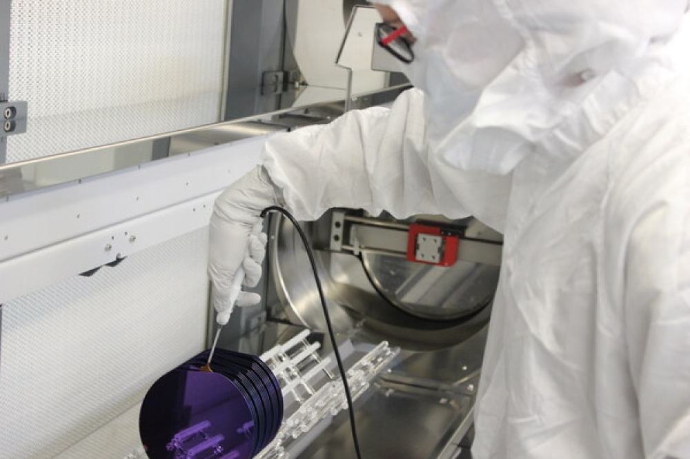
Cleanroom processing technologies for advanced usersProcess tolerance considerations for device designDevice simulation using commercial software packagesCircuit design using commercial PDK softwareCleanroom processes overview for non-technical staff membersHealth & safety in cleanroomsParticipants have the chance to visit Southampton’s cleanroom complex and experience live device fabrication using advanced, industry-compatible, deep-UV projection lithography and related tools.
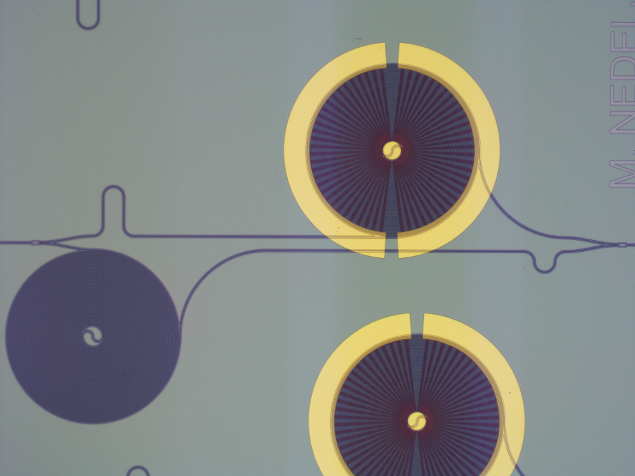
Training can be integrated into any of the CORNERSTONE MPW fabrication batches on various silicon-on-insulator (SOI) platforms, including state-of-the-art modulator design, fabrication and characterisation, or offered as a stand-alone course.
“At a higher level we are looking at options to continue enhancing what we offer at CORNERSTONE. Part of this applies to devices we fabricate and how that can apply to the courses and training that we provide… For example, we design our own electronic modulator drivers, and then we flip chip them onto the SiP, and this would allow us to offer electronic / photonic integration through CORNERSTONE. We also want to offer pick and place, and then more platforms that could be incorporated into SiP…We are developing a silicon nitride platform, an undercut silicon platform for mid infrared (MIR) applications, and a germanium on silicon platform that supports longer MIR wavelengths up to 14 µm. We would like users at CORNERSTONE to access as much of this technology as possible, so flexibility is a key to offer more, but without undercutting our partners or customers,” Reed remarked.
As he explained, the CORNERSTONE programme has grown rapidly; it is now onto its thirteenth call. “It’s a user driven process,” noted Reed. “It has taken off quite quickly – we have only been offering CORNERSTONE fabricated devices just over two years, and one thing that the users have said is that it’s a great program, but can you offer more platforms and functionality? We are looking for ways to offer things through CORNERSTONE which have been developed as part of our other research projects, and ways that we can expand the programme…But as complexities increase we have to be sure everything fits together.”
One recent participant that plans a return engagement in Southampton and the CORNERSTONE programme is Dr. Iain Crowe, Associate Professor in Electrical and Electronic Engineering at the University of Manchester (UK). Crowe utilized CORNERSTONE’s MPW programme after previously working with SiP foundries elsewhere in Europe and Asia.
“The facilities in Southampton are world class and the personnel highly professional and expert in silicon photonics. The CORNERSTONE programme has helped establish this facility as the UK leader in silicon photonics MPW fabrication, contributing to the successful delivery of a number of other (UK and internationally) funded research programs,” Crowe said.
An important aspect of Crowe’s work that was facilitated through CORNERSTONE was the design verification process that aided the efforts of students and faculty by ‘de-risking’ a number of their designs.
“We have used the facility now more than once and although these are prototyping runs for research purposes, as our understanding of certain designs matures we certainly will be considering how these can be scaled up for future manufacturing and will seek the support at the ORC to help us streamline this,” Crowe explained. “In fact, we have just submitted another set of designs as part of MPW number 12, which will be a crucial step in helping us to deliver our own EPSRC-GCRF funded contract.”
Accessing world-class facilities for research, product development and making the move to volume manufacturing requires high-quality materials as well as skilled expertise and the latest process tools. Stuart Edwards, Business Development Director at IQE, said he continues to be impressed with the range of services and expertise offered through CORNERSTONE. IQE manufactures advanced epitaxial wafers for a wide range of applications for wireless, optoelectronic, electronic and solar devices; the company is headquartered in Cardiff, Wales. IQE, with fabrication locations in the UK, the United States and Asia, said it sees the combination of services and training offered through CORNERSTONE as a key resource for building a UK/European integrated photonics industry.
“IQE has been involved in the development and supply of advanced epitaxy material for many years for use in the fabrication of silicon photonic devices, both for low TRL activities with universities and product level processes for commercial customers. As the field develops and continues to grow we are committed to remain a key supplier in the market and as part of this we were keen to leverage the benefits of the knowledge of Graham and his team in Southampton. After becoming aware of the CORNERSTONE programme and the options available for bespoke training, we are exploiting this across our development, operations and commercial teams to improve our focus in this area and better serve our customers.”
Looking ahead to the future of both photonic integration research and device design, Reed said that one of the most rewarding aspects of working through CORNERSTONE, and their many partners and customers, is the way that one product or device idea leads to another. Constant feedback and new ideas generated by MPW runs, as well as interaction with training course participants, drives the potential to expand what CORNERSTONE offers.
“We always look for ways to incorporate what we are doing in our own research into what we can offer through CORNERSTONE and MPW runs, but you have to get down to a much deeper level of detail. There are many ideas about what we might be able to offer and integrate, yet we need to make certain that we can fully develop these offerings and truly make them available, and this takes time…In principle some new things we try will work for our own applications or in the lab, but we want to make certain the process works for the majority of what our customers’ purposes might be and that all we offer is compatible,” he explained.
After more than 30 years in a field he helped pioneer, Reed looks forward to the continuing challenges, even though he finds that with the growth and expansion of the organization’s programmes, he’s more of an administrator than he might like to be on a given day. “In some fields one does his part, but seldom gets to see it from the start. I am fortunate in that I could help start a field and then get to watch it evolve; it’s all interesting stuff. I like to see something that we develop and then see how others take it in different directions or see different possibilities, like going to a conference where you hear a presentation and you realize it was something that started with our research…It’s quite amazing.”
“As you know, one of my former students, Dr. Andrew Rickman, went on to found Bookham Technology that’s now part of Lumentum. We worked with Bookham for more than a decade, but eventually they got out of SiP and I was wondering if ‘that was it’ around 2000. About two weeks later, Intel rang and said that they had a programme for silicon photonics, and that was the beginning of my work in their programme as a consultant. I saw what they were putting into it back then. After a while you realize that this thing—SiP—has legs to it after all.”

Indeed it has. CORNERSTONE has scheduled MPW runs throughout the year, with the next being on their SOI 500 nm platform with a June announcement of the design rules. This MPW run will be followed by a 220 nm SOI platform opportunity that has an August announcement. Check the organization’s website for further details at www.cornerstone.sotonfab.co.uk, or send an email to this address: cornerstone@soton.ac.uk.


