Soitec: Beyond Silicon-on-Insulator

Having just acquired EpiGaN, SOI manufacturer, Soitec, is set to take on 5G GaN power amplifier markets, reports Rebecca Pool.
Just last month, France-based manufacturer of silicon-on-insulator materials, Soitec, acquired EpiGaN, Belgium, for a hefty €30 million, adding to its growing suite of silicon-based and compound semiconductor technologies.
IMEC spin-off EpiGaN, has spent nearly a decade honing its GaN-on-silicon and GaN-on-SiC epiwafers. And as Soitec's head of strategy, Thomas Piliszczuk, puts it: “EpiGaN may be a start-up but the maturity of technology in their products is quite amazing, so with our support, we will be able move this forward very quickly.”
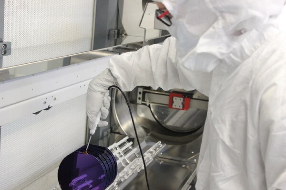
Soitec span out of CEA-LETI, Grenoble, in 1992 to manufacture SOI wafers on an industrial scale using its wafer-bonding and layer-splitting process called Smart Cut. Here, ultra-thin insulating single-crystal layers are implanted into surfaces and then transferred from one substrate to another to produce a SOI wafer.
Semiconductor manufacturers can then fabricate ICs onto the top layer of the SOI wafer to produce devices with, say, reduced parasitic capacitance.
Since this time, Soitec has continually ramped production, incorporated more materials into its Smart Cut process, including GaN, and today produces a range of engineered substrates for power and RF applications.
For example, digital SOI products include a fully depleted SOI – FD-SOI - with an ultrathin top silicon layer on which to build low power chips for, say, base stations and handsets.
Meanwhile, RF-SOI includes enhanced-Signal Integrity substrates with a trap-rich layer for LTE and LTE-Advanced front-end module ICs.
But while SOI products make up some 95% of Soitec's business right now – the company recently signed several long-term supply agreements for 300 mm SOI wafers with Global Foundries – it has been eyeing opportunities beyond SOI for some time.
As Piliszczuk points out: “SOI is no longer a niche market and we have been growing more and more, so over the last few years we have made the first steps beyond SOI.”
“For example, we develop engineering substrates using piezoelectric materials and are ramping up production of Piezoelectric on Insulator for RF filters while working with all the key RF companies,” he says.
What's more, the company has honed it Smart Cut process to transfer a thin layer of crystalline material from a GaN or InP donor substrate to another substrate to produce a cost-effective compound semiconductor wafer.
“We're engaged with key micro-LED makers to provide these substrates for devices and see huge opportunities here,” says Piliszczuk. “We've been looking at GaN for some time and believe this technology has reached a point where it can bring in substantial business, especially for 5G.”
But, Soitec doesn't intend to stop at GaN. According to Piliszczuk, the company has also been eyeing SiC opportunities for some time.
“Silicon carbide is a big opportunity and we are being pulled heavily by end-customers who believe we can bring lots of value here,” he says. “Supply of silicon carbide is a huge challenge but with Smart Cut we could take a silicon carbide crystal, cut a thin layer and transfer this onto a [receiving] substrate and in this way generate a much bigger supply... so we are working very heavily on silicon carbide projects.”
A future with EpiGaN
From here on in, EpiGaN is set to play a critical role for Soitec.
Soitec's current line of SOI and POI products meet the demands of many of the key components critical to 5G base station and handset architecture, such as transceivers, low noise amplifiers, antenna switches filters and more.
However, with EpiGaN's GaN-on-silicon and GaN-on-SiC epiwafers the company can now make a play for power amplifier markets in both base stations and handsets.
Indeed, GaAs is currently the mainstream technology for power amplifiers in 4G and many 5G handsets, but GaN is making in-roads into 5G mmW markets. With EpiGaN, Soitec can also exploit this development.
“We first approached EpiGaN last year - we have a big offering of engineered substrates in 5G RF markets but also saw the big potential for GaN here too” says Piliszczuk. “We realised that by combining EpiGaN's technology with our market position and manufacturing scale would bring many opportunities.”
With the acquisition secured, Soitec first intends to fully integrate EpiGaN into its company. As Piliszczuk says: “We will do this step by step but we want this to be the same business as Soitec.”
The company then intends to ramp production at EpiGaN's production site in Hasselt, Belgium. Indeed, the former start-up recently purchased an Aixtron G5 reactor, which is currently being installed and qualified.
According to Piliszczuk, Soitec will add to this reactor, and also buy other process control and cleaning tools in the coming months. “There is enough space for additional tools and we are confident that we can use this space,” he says.
And in a similar vein, Soitec will continue to move EpiGaN's epi-wafers from six inch to eight inch production. “We want to make sure this project moves to the required level of maturity very quickly, and in the long-term we may need another production site,” highlights Piliszczuk.
“RF 5G as well as power electronics markets are just growing and growing... but to a certain extent GaN businesses are vertically organised,” he adds. “We believe this set-up is going to break, and our discussions with EpiGaN customer prove it - so we are confident we are now very well positioned to support these markets.”


