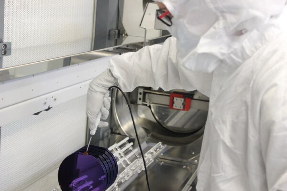
Nanoscribe Expands Portfolio with New GT2 High-Resolution 3D Printing Solution

Nanoscribe’s new GT2 can print filigree structures up to the millimeter range with extremely high resolution.
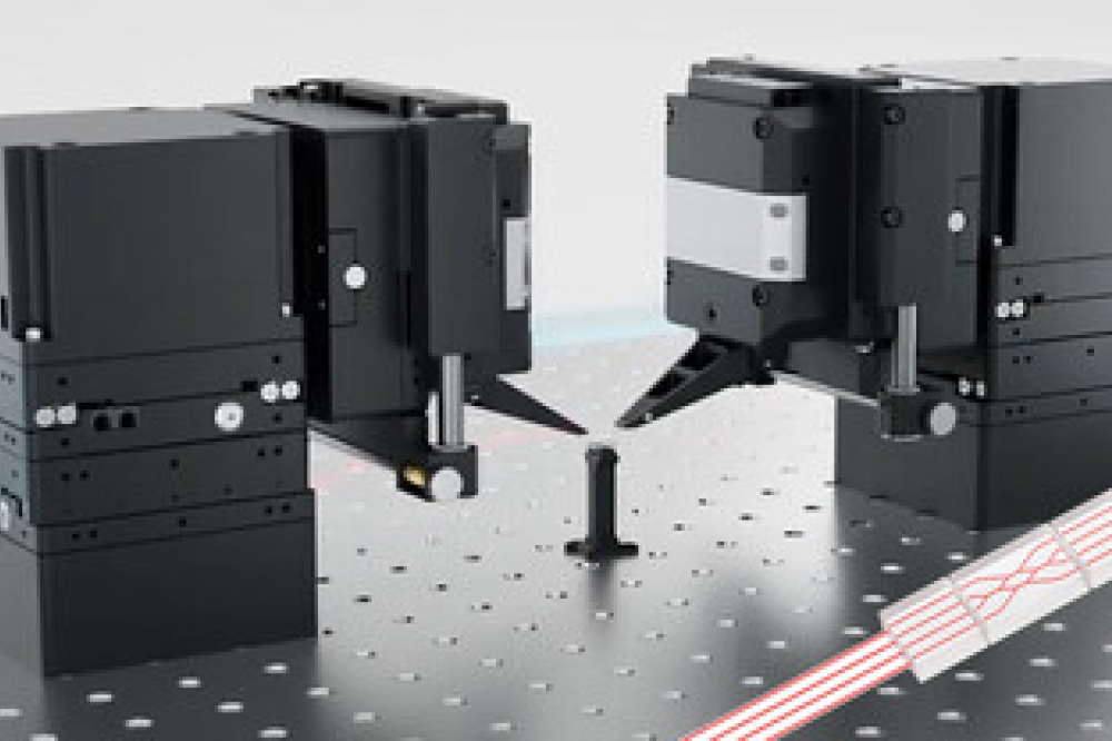
Nanoscribe (Germany) has enhanced its lineup of micrometer precision 3D printers with the introduction of its new Photonic Professional GT2 microfabrication system. The high-resolution 3D printers add additional capabilities including expanded printing range up to the millimeter scale as well as industry-oriented features for ‘maskless’ lithography.
According to Nanoscribe CEO Martin Hermatschweiler, hardware optimizations and software components as well as the company’s IP-Q printing materials developed for high volume applications were key to enabling the company’s latest 3D printer release.
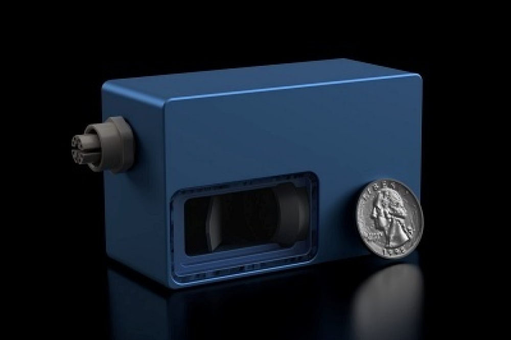
Figure 1: The Nanoscribe Photonic Professional GT2 system is shown above. The company’s new 3D printer enables the production of larger structures with high precision more quickly than competing solutions.
“High resolution microstructures up to a height of 8mm can now be produced for the first time. While Nanoscribe devices have always been optimally suited to the additive production of the most detailed structures, objects with sub-micrometer details from (typically) 160 nanometers up to the millimeter range on a printing area of up to 100x100 mm² can now be produced in a very short time,” he remarked.
Depending on the desired size and resolution, users can choose from sets of objectives, substrates, materials, and automated processes tailored to their applications. The user-friendly 3D printing workflow enables the fabrication of individual elements with maximum shape accuracy and surface smoothness, meeting the requirements for microlenses in the smartphone industry or filigree scaffold structures utilized in cellular biology. Likewise, high-precision masters can be produced for molding processes in series production on a scale and with a degree of design freedom that cannot be achieved with alternative subtractive nor additive manufacturing technologies.
“The extension of the maximum print volumes toward the macroscale was a ‘great wish’ of our customers and project partners from industry,” said Hermatschweiler. “With this update of our extremely successful generation of Photonic Professional devices, we have now succeeded in overcoming previous physical limitations while increasing the performance of the devices by a factor of up to 10 in terms of productivity and speed,” he added.
“At Nanoscribe, we believe that our technology is perfectly suited to address the challenges faced by photonic designers and others working at nano-scale thanks to the tremendous flexibility of additive micro-printing. Our technology allows placing micro-structures with very high accuracy - some of our costumers routinely place optical elements with sub-100 nm accuracy. Combined with very small sub-micron feature sizes and surface roughness better than 10 nm, such precision naturally enables completely new solutions in photonic packaging,” he explained.
“Our driving goal is providing the best tools on the market to our customers from academia and industry which we believe will enable them to successfully develop 3D printed nano- and microstructures. We provide comprehensive support ranging from material development over fabrication support to design advice. In fact, several of our employees come from an integrated photonics, packaging and micro-optics background,” he added.
Extended Range of Industry Applications
Hermatschweiler said that Nanoscribe’s new Photonic Professional GT2 3D printer can significantly shorten product development cycles, especially in cases where large-volume structures in the millimeter range are required, such as for microfluidic elements (filters or nozzles), lab-on-a-chip applications, or micro rapid prototyping. In the field of sensor and actuator technology, various product components can now be printed quickly and precisely on MEMS components or silicon chips without further adjustment or assembly processes thanks to the variety of printable substrates. Photonic Professional GT2 systems will also open up new possibilities in the field of medical technology, such as the direct printing of micro-optics on glass fibers for minimally invasive endoscopes or for the manufacture of microneedles for painless drug delivery through the skin.
Functional Principle of Two-Photon Polymerization in 3D Printing
Nanoscribe systems combine the technology of two-photon polymerization with the workflow of a conventional 3D printing process. Their system utilizes a precisely focused femtosecond laser to cure a photosensitive material layer-by-layer. In a simple workflow, software especially developed for the printing process supports the import of CAD models with extensive configuration options, including a wide selection of preset parameters. A 3D preview as well as a real-time camera monitoring supports users seeking optimal adjustment and monitoring of the 3D printing process.
Nanoscribe’s proprietary software programs (DeScribe and NanoWrite) have been enhanced for the company’s latest Photonic Professional GT2 printer generation. Up to 10-times higher printing speeds can be achieved with the system’s intelligent printing strategies. Thanks to enormous design freedom, Nanoscribe printers can produce structures of varying complexity: for example, grating-like high resolution photonic structures in 2D, hemispherical microlenses with vertical slopes in 2.5D, and complex 3D objects such as gas-dynamic micronozzles can all be printed through nano-scale additive manufacturing. Parts printed with replicable topographies can also serve as polymer masters for molding processes. Using galvanic processes, 3D printed polymer masters can be metallized in order to be used as nickel shims for mass production utilizing industry-standard injection molding processes.
According to Nanoscribe, the company’s two-photon polymerization is best qualified amongst competing solutions for creating the most detailed, finely-crafted structures on the micro- and mesoscale. While other 3D printing technologies, such as Polyjet, DLP (Digital Light Processing), or SLA (stereolithography), excel from the centimeter range, the strengths of Photonic Professional GT2 systems lie in its ability to create device structures utilizing ultra-precise 3D microfabrication.
A complete System
Nanoscribe also announced its new IP-Q Photoresin to complement the introduction of its Photonic Professional GT2 print system. In the Nanoscribe IP Photoresin portfolio there are suitable options for varying requirements, such as submicron features, overhanging elements, optical-quality surfaces or high-speed microfabrication up to the macroscale. The Photonic Professional GT2 printers work as open systems for a broad range of materials. The IP resins are exclusively designed and optimized for two-photon polymerization (2PP) and their use with Nanoscribe’s 3D printers.
Nanoscribe has already partnered with a multitude of manufacturers, research institutes and universities that are seeking new approaches to creating advanced photonic and semiconductor device structures utilizing additive manufacturing.
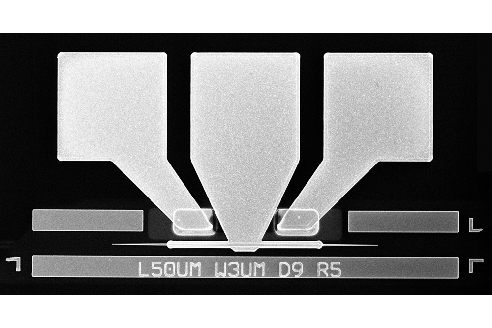
For example, the Dutch research institute AMOLF has developed and fabricated a 3D nanophotonic lens in collaboration with the Western University in Canada and the City University of New York (USA.) Using a Photonic Professional System from Nanoscribe, the researchers printed an extremely small lens on top of a gallium arsenide nanowire, which is only 80 nm thick and acts as a light emitter. This way, the combination of a nanolens and a nanowire enables focused light emission, compared to an almost uniform emission of the nanowire itself.

Figure 2: Dutch researchers at AMOLF have developed and fabricated a 3D nanophotonic lens in collaboration with researchers in Canada and the US using a Nanoscribe Photonic Professional System. The researchers printed an extremely small lens on top of a gallium arsenide (GaAs) nanowire, which is only 80 nm thick and acts as a light emitter.
The researchers at AMOLF believe that highly direction-sensitive nanoscale emitters and sensors offer potential in many applications. This includes optical quantum computers as well as solar cells with nanoscale structured areas or surfaces. However, the enhancement of directivity on nanoscale devices is a major technical challenge. In this work, the researchers applied an evolutionary algorithm to design a complex 3D geometry with sub-wavelength features down to nearly 200 nm. This 3D design utilizes nanoscale interference effects to achieve its high directivity.
For more information about Nanoscribe 3D micro-printing solutions, visit the company’s website at: www.nanoscribe.com


