
A Glimpse into the Future
UCSB engineering professor John Bowers’ group develops a high-performance quantum dot mode-locked laser on silicon
“The level of data traffic in the world is going up very, very fast,” said Bowers, co-author of a paper on the new technology in the journal Optica. Generally speaking, he explained, the transmission and data capacity of state-of-the-art telecommunications infrastructure must double roughly every two years to sustain high levels of performance. That means that even now, technology companies such as Intel and Cisco have to set their sights on the hardware of 2024 and beyond to stay competitive.
Enter the Bowers Group’s high-channel-count, 20 gigahertz, passively mode-locked quantum dot laser, directly grown — for the first time, to the group’s knowledge — on a silicon substrate. With a proven 4.1 terabit-per-second transmission capacity, it leaps an estimated full decade ahead from today’s best commercial standard for data transmission, which is currently reaching for 400 gigabits per second on Ethernet.
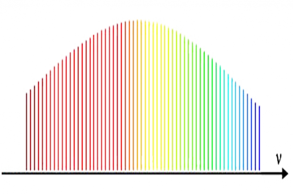
The technology is the latest high-performance candidate in an established technique called wavelength-division-multiplexing (WDM), which transmits numerous parallel signals over a single optical fiber using different wavelengths (colors). It has made possible the streaming and rapid data transfer we have come to rely on for our communications, entertainment and commerce.
The Bowers Group’s new technology takes advantage of several advances in telecommunications, photonics and materials with its quantum dot laser — a tiny, micron-sized light source — that can emit a broad range of light wavelengths over which data can be transmitted.
“We want more coherent wavelengths generated in one cheap light source,” said Songtao Liu, a postdoctoral researcher in the Bowers Group and lead author of the paper. “Quantum dots can offer you wide gain spectrum, and that’s why we can achieve a lot of channels.” Their quantum dot laser produces 64 channels, spaced at 20 GHz, and can be utilized as a transmitter to boost the system capacity.
The laser is passively ‘mode-locked’ — a technique that generates coherent optical ‘combs’ with fixed-channel spacing — to prevent noise from wavelength competition in the laser cavity and stabilize data transmission.
This technology represents a significant advance in the field of silicon electronic and photonic integrated circuits, in which the primary goal is to create components that use light (photons) and waveguides — unparalleled for data capacity and transmission speed as well as energy efficiency — alongside and even instead of electrons and wires. Silicon is a good material for the quality of light it can guide and preserve, and for the ease and low cost of its large-scale manufacture. However, it’s not so good for generating light.
“If you want to generate light efficiently, you want a direct band-gap semiconductor,” said Liu, referring to the ideal electronic structural property for light-emitting solids. “Silicon is an indirect band-gap semiconductor.” The Bowers Group’s quantum dot laser, grown on silicon molecule-by-molecule at UC Santa Barbara’s nanofabrication facilities, is a structure that takes advantage of the electronic properties of several semiconductor materials for performance and function (including their direct band-gaps), in addition to silicon’s own well-known optical and manufacturing benefits.
This quantum dot laser, and components like it, are expected to become the norm in telecommunications and data processing, as technology companies seek ways to improve their data capacity and transmission speeds.
“Data centers are now buying large amounts of silicon photonic transceivers,” Bowers pointed out. “And it went from nothing two years ago.”
Since Bowers a decade ago demonstrated the world’s first hybrid silicon laser (an effort in conjunction with Intel), the silicon photonics world has continued to create higher efficiency, higher performance technology while maintaining as small a footprint as possible, with an eye on mass production. The quantum dot laser on silicon, Bowers and Liu say, is state-of-the-art technology that delivers the superior performance that will be sought for future devices.
“We’re shooting far out there,” said Bowers, who holds the Fred Kavli Chair in Nanotechnology, “which is what university research should be doing.”
Research on this project was also conducted by Xinru Wu, Daehwan Jung, Justin Norman, MJ Kennedy, Hon K. Tsang and Arthur C. Gossard at UC Santa Barbara.

John Bowers, left, and Songtao Liu Photo Credit: Sonia Fernandez


