NASA Team Investigates Ultrafast Laser Machining for Multiple Spaceflight Applications
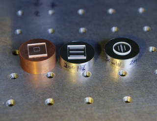
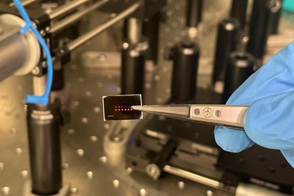
A Goddard team is using an ultrafast laser to bond dissimilar materials, with the goal of ultimately eliminating epoxies that outgas and contaminate sensitive spacecraft components. Shown here are a few samples (from left to right): silica welded to copper; silica welded to Invar; and sapphire welded to Invar.
An ultrafast laser that fires pulses of light just 100 millionths of a nanosecond in duration could potentially revolutionize the way that NASA technicians manufacture and ultimately assemble instrument components made of dissimilar materials.
A team of optical physicists at NASA’s Goddard Space Flight Center in Greenbelt, Maryland, is experimenting with a femtosecond laser and has already shown that it can effectively weld glass to copper, glass to glass, and drill hair-sized pinholes in different materials.
Now the group, led by optical physicist Robert Lafon, is expanding its research into more exotic glass, such as sapphire and Zerodur, and metals, such as titanium, Invar, Kovar, and aluminum — materials often used in spaceflight instruments. The goal is to weld larger pieces of these materials and show that the laser technology is effective at adhering windows onto laser housings and optics to metal mounts, among other applications.
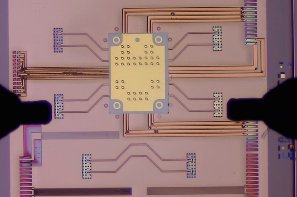
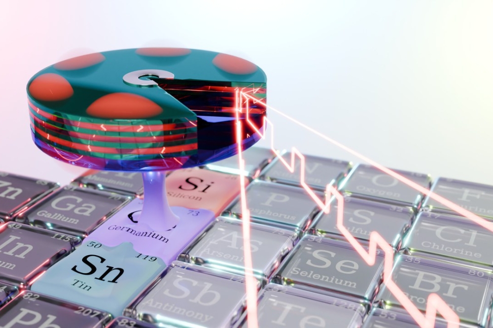
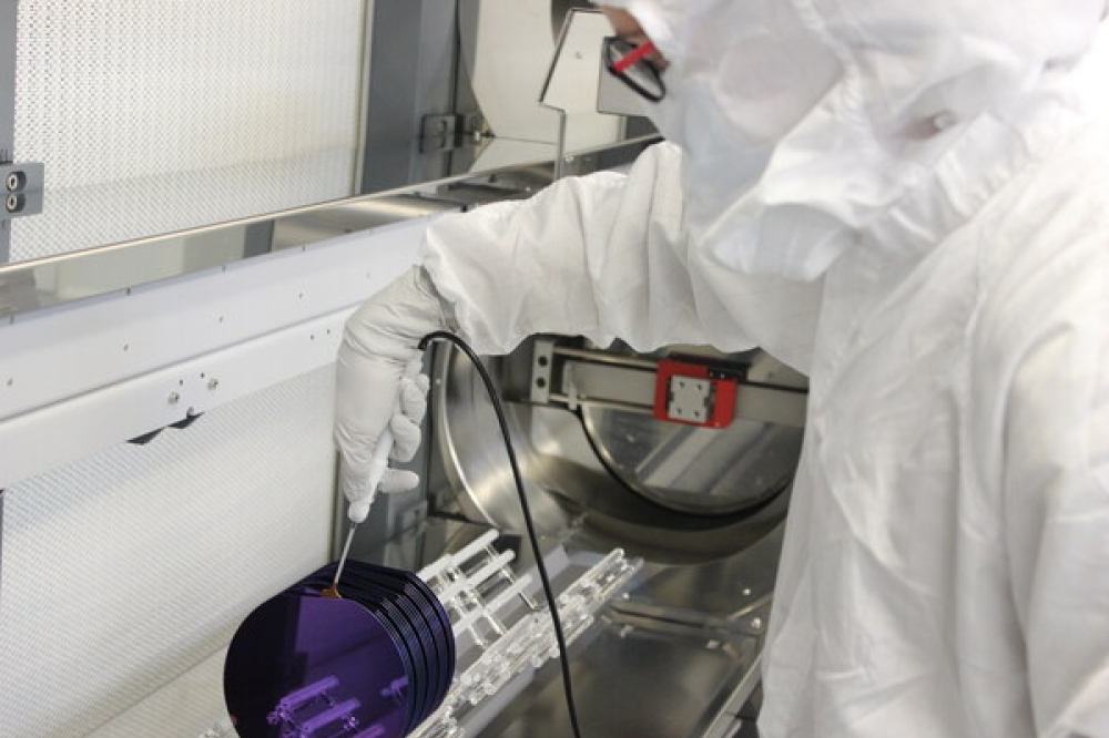
With support from the Space Technology Mission Directorate’s Center Innovation Fund program, the group is also exploring the technology’s use in fabricating and packaging photonic integrated circuits, an emerging technology that could benefit everything from communications and data centers to optical sensors. Though they are similar to electronic integrated circuits, photonic integrated circuits are fabricated on a mixture of materials, including silica and silicon, and use visible or infrared light, instead of electrons, to transfer information.
“This started as pure research, but now we hope to start applying what we have learned to the fabrication of instruments here at Goddard,” Lafon said, referring to the work he and his team, including Frankie Micalizzi and Steve Li, are using to experiment with different materials and techniques that could benefit spaceflight applications. “We already see what the applications could be. In this case, research for research’s sake is in our best interests,” Lafon said.
The Technology’s Virtues
Laser team
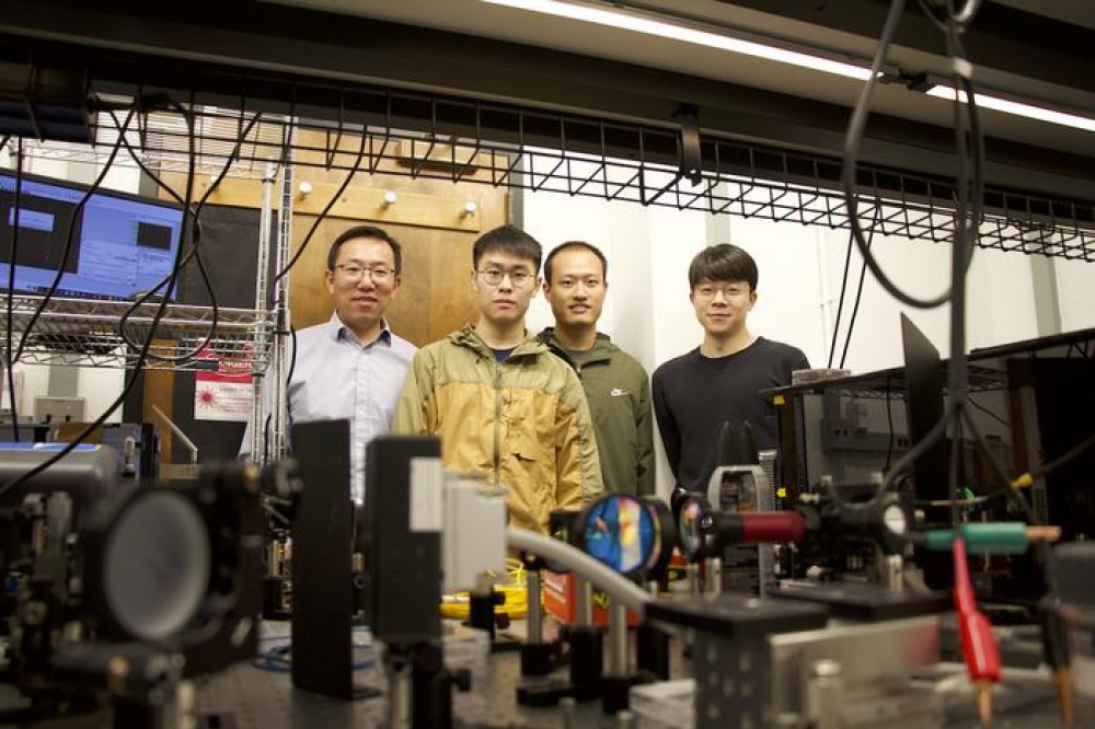
Steve Li (left), Frankie Micalizzi (middle), and Robert Lafon (right) are using an ultrafast laser to bond dissimilar materials and etch microscopic channels or waveguides through which light could travel in photonic integrated circuits and laser transmitters. (Photo Credit: Bill Hrybyk/NASA) Credits: NASA/W. Hrybyk
Central to advancing these applications is the laser itself. By virtue of its short pulses — measured at one quadrillionth of a second — an ultrafast laser interacts with materials in a unique way, Lafon said. The laser energy doesn’t melt the targeted material. It vaporizes it without heating the surrounding matter.
As a result, technicians can precisely target the laser and bond dissimilar materials that otherwise couldn’t be attached without epoxies. “It’s not possible to bond glass to metal directly,” Lafon said. “You have to use epoxy, which outgases and deposits contaminants on mirrors and other sensitive instrument components. This could be a serious application. We want to get rid of epoxies. We have already begun reaching out to other groups and missions to see how these new capabilities might benefit their projects.”
Another important application is in the area of micromachining. “The ability to remove small volumes of material without damaging the surrounding matter allows us to machine microscopic features,” Lafon added.
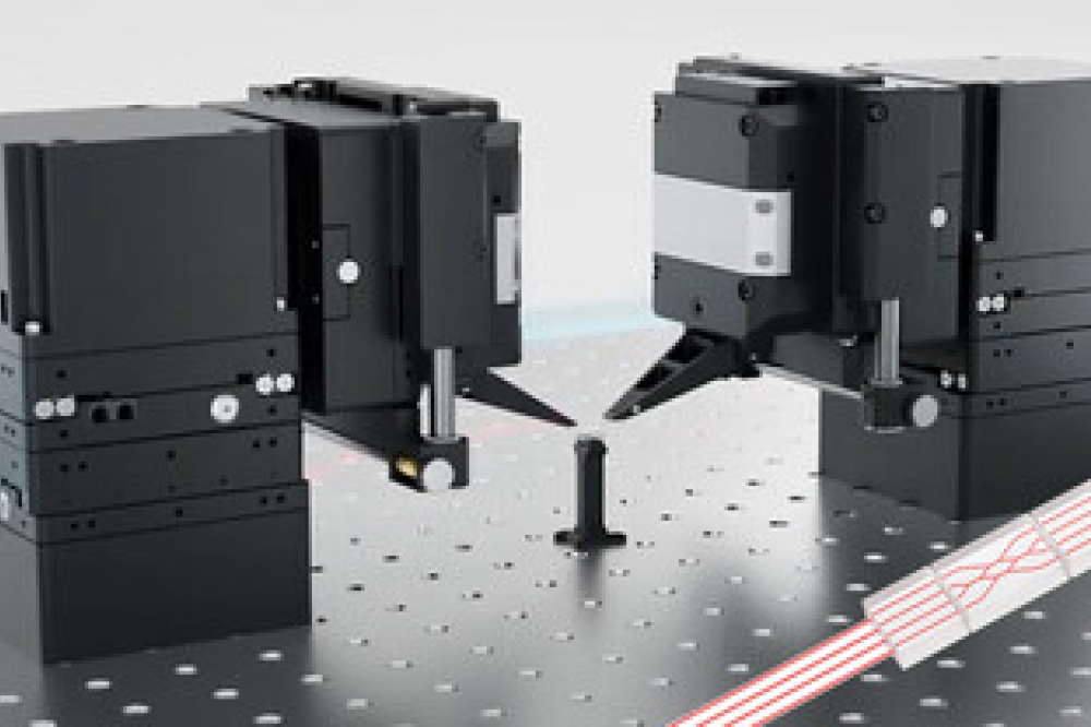
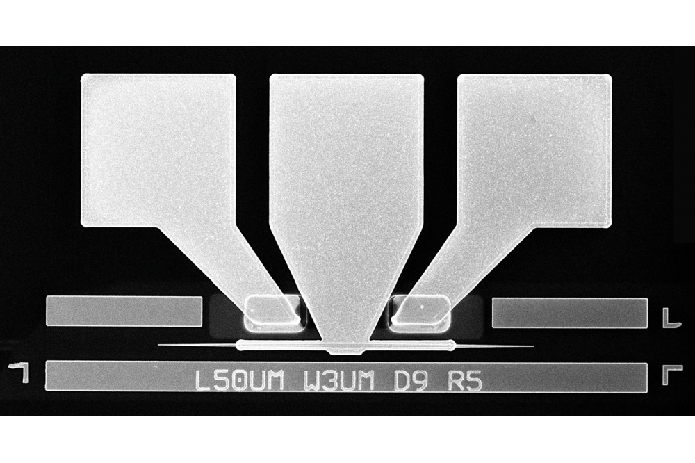
Microscopic features include everything from drilled, hair-sized pinholes in metals — an application the team already demonstrated — to etching microscopic channels or waveguides through which light could travel in photonic integrated circuits and laser transmitters. The same waveguides could allow liquids to flow through microfluidic devices and chips needed for chemical analyses and instrument cooling.
Widespread Applicability to NASA Projects
“Ultrafast lasers offer fundamental changes in how we can microprocess materials,” said Ted Swanson, senior technologist for strategic integration at Goddard. “The team’s work on this research effort will allow Goddard to adapt this emerging technology to a wide variety of flight applications.”
To that end, the team — between working on several of NASA’s high-profile laser communications projects, including the Laser Communications Relay Demonstration — plans to compile a library of micromachining and welding capabilities. “Once we are able to demonstrate this capability reliably, we will attempt to apply it to existing challenges here at Goddard. Our initial research is showing that this technology could be applied to a large number of projects across NASA,” Lafon said.


